ST BlueNRG-LP可编蓝牙低功耗无线SoC开发方案
 75
75
 拍明
拍明
原标题:ST BlueNRG-LP可编蓝牙低功耗无线SoC开发方案
ST公司的BlueNRG-LP是超低功耗可编蓝牙低功耗无线系统级芯片(SoC),包括有该公司的最新2.4GHz RF无线电IP和无可比拟的性能和极长的电池寿命.器件和蓝牙低功耗SIG核指标V5.1点对点连接以及蓝牙网状Bluetooth Mesh网兼容,允许大量设备以可靠方式建立起网络. BlueNRG-LP还适用于2.4GHz无线通信,提供超低等候的应用. BlueNRG-LP嵌入了Cortex®-M0+ MCU,工作频率高达64MHz,和一个基于DMA的BlueNRG核协处理器.蓝牙数据速率2MHz和长距离((Coded PHY),通路选择算法#2,GATT缓存,RX灵敏度为-97 dBm @ 1 Mbps和 -104 dBm @ 125 kbps(长距离),可编输出功率高达+8dBm,数据速率支持2 Mbps, 1 Mbps, 500 kbps 和125 kbps,集成了平衡不平衡转换器,支持外接功率放大器(PA),工作电压从1.7V到3.6V,工作温度-40 C 到105 C.主要用在工业,家庭和工业自动化,智能照明,健美,健身和运动,保健消费类医疗设备,遥控,养老设施,手机外设以及PC外设.本文介绍了BlueNRG-LP主要特性,框图和系统架构图,总线矩阵图,RF框图和多种应用框图,以及开发板STEVAL-IDB011V1主要特性,电路图和材料清单.
The BlueNRG-LP is an ultra-low power programmable Bluetooth® Low Energy
wireless SoC solution. It embeds stmicroelectronicss state-of-art 2.4 GHz RF radio
IPs combining unparalleled performance with extremely long-battery lifetime. It is
compliant with Bluetooth® Low Energy SIG core specification version 5.1 addressing
point-to-point connectivity and Bluetooth Mesh networking and allows large-scale
device networks to be established in a reliable way. The BlueNRG-LP is also suitable
for 2.4 GHz proprietary radio wireless communication to address ultra-low latency
applications.
The BlueNRG-LP embeds a Cortex®-M0+ microcontroller that can operate up to 64
MHz and also the BlueNRG core coprocessor (DMA based) for Bluetooth Low
Energy timing critical operations.
The main Bluetooth® Low Energy 5.1 specification supported features are:
2 Mbps data rate, long range (Coded PHY), advertising extensions, channel selection
algorithm #2, GATT caching, hardware support for simultaneous connection, master/
slave and multiple roles simultaneously, extended packet length support.
In addition, the BlueNRG-LP provides enhanced security hardware support by dedicated hardware functions:
True random number generator (RNG), encryption AES maximum 128-bit security
co-processor, public key accelerator (PKA), CRC calculation unit, 48-bit unique ID,
Flash memory read and write protection.
The BlueNRG-LP can be configured to support standalone or network processor
applications. In the first configuration, the BlueNRG-LP operates as single device in
the application for managing both the application code and the Bluetooth Low Energy
stack.
The BlueNRG-LP embeds high-speed and flexible memory types:
Flash memory of 256 kB, RAM memory of 64 kB, one-time-programmable (OTP)
memory area of 1 kB, ROM memory of 7 kB.
Direct data transfer between memory and peripherals and from memory-to-memory
is supported by eight DMA channels with a full flexible channel mapping by the
DMAMUX peripheral.
The BlueNRG-LP embeds a 12-bit ADC, allowing measurements of up to eight
external sources and up to three internal sources, including battery monitoring and a
temperature sensor.
The BlueNRG-LP has a low-power RTC and one advanced 16-bit timer.
The BlueNRG-LP features standard and advanced communication interfaces:
1x SPI, 2x SPI/I2S, 1x LPUART, 1x USART supporting ISO 7816 (smartcard mode),
IrDA and Modbus mode, 2x I2C supporting SMBus/PMBus, 1x channel PDM.
The BlueNRG-LP operates in the -40 to +105 C (+125 C junction) temperature range from a 1.7 V to 3.6 V power supply. A comprehensive set of power-saving modes enables the design of low-power applications.
The BlueNRG-LP integrates a high efficiency SMPS step-down converter and an
integrated PDR circuitry with a fixed threshold that generates a device reset when the
VDD drops under 1.65 V.
The BlueNRG-LP comes in different package versions supporting up to:
32 I/Os for the QFN48 package, 20 I/Os for the QFN32 package, 30 I/Os for the
WCSP49 package.
BlueNRG-LP主要特性:
• Bluetooth Low Energy system-on-chip supporting Bluetooth 5.1 specifications
– 2 Mbps data rate
– Long range (Coded PHY)
– Advertising extensions
– Channel selection algorithm #2
– GATT caching
• Radio
– RX sensitivity level: -97 dBm @ 1 Mbps, -104 dBm @ 125 kbps (long range)
– Programmable output power up to +8 dBm (at antenna connector)
– Data rate supported: 2 Mbps, 1 Mbps, 500 kbps and 125 kbps
– Integrated balun
– Support for external PA
– BlueNRG core coprocessor (DMA based) for Bluetooth Low Energy timing critical operation
– 2.4 GHz proprietary radio driver
– Suitable for systems requiring compliance with the following radio frequency regulations: ETSI EN 300 328, EN 300 440, FCC CFR47 part 15, ARIB STD-T66
• Ultra-low power radio performance
– 10 nA in SHUTDOWN mode (1.8 V)
– 0.6 uA in DEEPSTOP mode (with external LSE and BLE wake-up sources, 1.8 V)
– 0.9 uA in DEEPSTOP mode (with internal LSI and BLE wake-up sources, 1.8 V)
– 4.3 mA peak current in TX (@ 0 dBm, 3.3 V)
– 3.4 mA peak current in RX (@ sensitivity level, 3.3V)
• High performance and ultra-low power Cortex-M0+ 32-bit, running up to 64 MHz
• Dynamic current consumption: 18 μA/MHz
• Operating supply voltage: from 1.7 to 3.6 V
• -40 C to 105 C temperature range
• Supply and reset management
– High efficiency embedded SMPS step-down converter with intelligent bypass mode
– Ultra-low power power-on-reset (POR) and power-down-reset (PDR)
– Programmable voltage detector (PVD)
• Clock sources
– Fail safe 32 MHz crystal oscillator with integrated trimming capacitors
– 32 kHz crystal oscillator
– Internal low-power 32 kHz RO
• On-chip non-volatile Flash memory of 256 kB
• On-chip RAM of 64 kB or 32 kB
• One-time-programmable (OTP) memory area of 1 kB
• Embedded UART bootloader
• Ultra-low power modes with or without timer and RAM retention
• Quadrature decoder
• Enhanced security mechanisms such as:
– Flash read/write protection
– SWD disabling
– Secure bootloader
• Security features
– True random number generator (RNG)
– Hardware encryption AES maximum 128-bit security co-processor
– HW public key accelerator (PKA)
– CRC calculation unit
– 48-bit unique ID
• System peripherals
– 1x DMA controller with 8 channels supporting ADC, SPI, I2C, USART and LPUART
– 1x SPI
– 2x SPI/I2S
– 2x I2C (SMBus/PMBus)
– 1x PDM (digital microphone interface)
– 1x LPUART
– 1x USART (ISO 7816 smartcard mode, IrDA, SPI Master and Modbus)
– 1x independent WDG
– 1x real time clock (RTC)
– 1x independent SysTick
– 1x 16-bit, 6 channel advanced timer
• Up to 32 fast I/Os
– 28 of them with wake-up capability
– 31 of them 5 V tolerant
• Analog peripherals
– 12-bit ADC with 8 input channels, up to 16 bits with a decimation filter
– Battery monitoring
– Analog watchdog
– Analog Mic I/F with PGA
• Development support
– Serial wire debug (SWD)
– 4 breakpoints and 2 watchpoints
• All packages are ECOPACK2 compliant
BlueNRG-LP应用:
• Industrial
• Home and industrial automation
• Smart lighting
• Fitness,wellness and sports
• Healthcare, consumer medical
• Security/proximity
• Remote control
• Assisted living
• Mobile phone peripherals
• PC peripherals
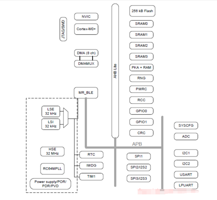
图1. BlueNRG-LP框图
系统架构图:
The main system consists of 32-bit multilayer AHB bus matrix that interconnects:
• Three masters:
– CPU (Cortex®-M0+) core S-bus
– DMA1
– Radio system
• Nine slaves:
– Internal Flash memory on CPU (Cortex®-M0+) S bus
– Internal SRAM0 (16 kB)
– Internal SRAM1 (16 kB)
– Internal SRAM2 (16 kB)
– Internal SRAM3 (16 kB)
– APB0 peripherals (through an AHB to APB bridge)
– APB1 peripherals (through an AHB to APB bridge)
– AHB0 peripherals
– AHBRF including AHB to APB bridge and radio peripherals (connected to APB2)
The bus matrix provides access from a master to a slave, enabling concurrent access and efficient operation even when several high-speed peripherals work simultaneously.
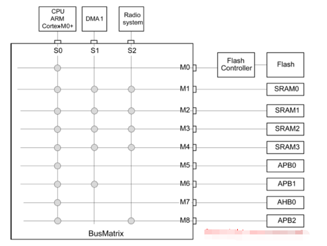
图2. BlueNRG-LP总线矩阵图
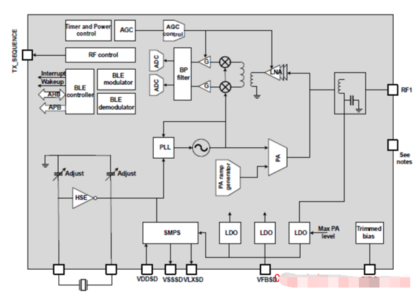
图3. BlueNRG-LP RF框图
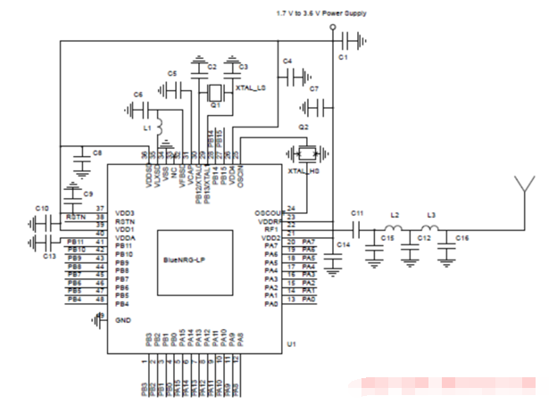
图4. BlueNRG-LP应用电路:DC/DC转换器,QFN48封装
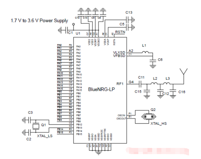
图5. BlueNRG-LP应用电路:DC/DC转换器,WCSP49封装
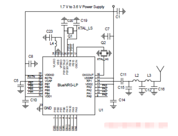
图6. BlueNRG-LP应用电路:DC/DC转换器,QFN432封装
BlueNRG-LP开发板STEVAL-IDB011V1
The BlueNRG-LP device is a low power Bluetooth® system-on-chip, compliant with the Bluetooth® specification and supports master, slave and simultaneous master-and-slave roles. The device also supports the Bluetooth Low Energy data length extension feature, 2 Mbps, Long Range and extended advertising features.
The following BlueNRG-LP kit is available:
• STEVAL-IDB011V1 QFN48 package development platform
The STEVAL-IDB011V1 development platform embeds a CMSIS-DAP programming/debugging interface and features hardware resources for a wide range of application scenarios: sensor data (accelerometer, pressure and temperature sensor), human interface (buttons and LEDs), digital MEMS microphone and serial communication through USB virtual COM. Three power options are available (USB only, battery only and external power supply plus USB) for high application development and testing flexibility.

图7. 开发板STEVAL-IDB011V1外形图
开发板STEVAL-IDB011V1包括:
• a BlueNRG-LP QFN48 package development platform
• a 2.4 GHz Bluetooth antenna
• a USB cable
The STEVAL-IDB011V1 development kit lets you experiment with BlueNRG-LP system on chip functions.
开发板STEVAL-IDB011V1主要特性:
• Bluetooth® low energy board based on the BlueNRG-LP Bluetooth low energy system-on-chip (QFN48 package)
• Associated development kit SW package (STSW-BNRGLP-DK) including firmware and documentation
• Bluetooth® low energy compliant, supports master, slave and simultaneous master-and-slave roles
• PCB antenna and option for adding a U.FL connector for antenna or measuring equipment
• 3 user LEDs
• 2 user buttons
• 3D digital accelerometer and 3D digital gyroscope
• MEMS pressure sensor with embedded temperature sensor
• MEMS audio sensor omnidirectional digital microphone
• Battery holder
• CMSIS-DAP debugger/programmer via micro USB connector
• USB to serial bridge to create an I/O channel with the BlueNRG-LP device
• Jumper to measure BlueNRG-LP current
• RoHS complian
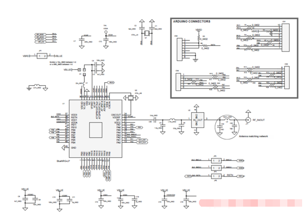
图8. 开发板STEVAL-IDB011V1电路图(1)
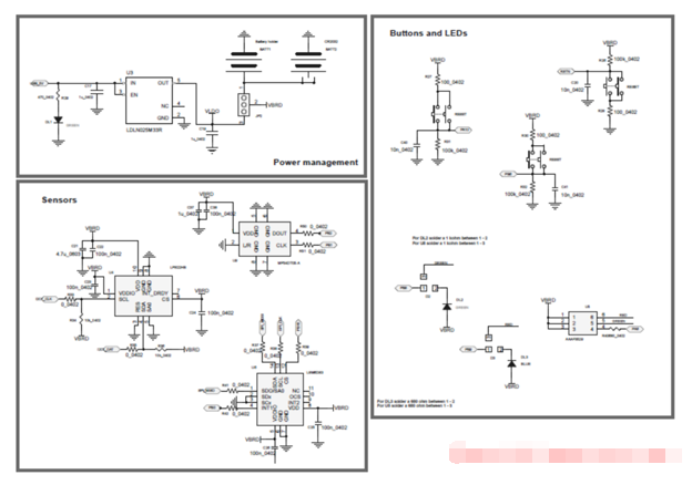
图9. 开发板STEVAL-IDB011V1电路图(2)
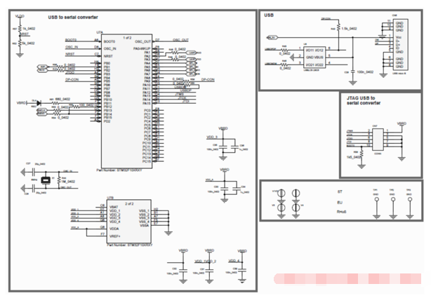
图10. 开发板STEVAL-IDB011V1电路图(3)
责任编辑:David
【免责声明】
1、本文内容、数据、图表等来源于网络引用或其他公开资料,版权归属原作者、原发表出处。若版权所有方对本文的引用持有异议,请联系拍明芯城(marketing@iczoom.com),本方将及时处理。
2、本文的引用仅供读者交流学习使用,不涉及商业目的。
3、本文内容仅代表作者观点,拍明芯城不对内容的准确性、可靠性或完整性提供明示或暗示的保证。读者阅读本文后做出的决定或行为,是基于自主意愿和独立判断做出的,请读者明确相关结果。
4、如需转载本方拥有版权的文章,请联系拍明芯城(marketing@iczoom.com)注明“转载原因”。未经允许私自转载拍明芯城将保留追究其法律责任的权利。
拍明芯城拥有对此声明的最终解释权。


 产品分类
产品分类




 2012- 2022 拍明芯城ICZOOM.com 版权所有 客服热线:400-693-8369 (9:00-18:00)


