


 产品分类
产品分类
ADI ADP2442 1A同步降压稳压器设计方案
 153
153
 拍明
拍明
原标题:ADI ADP2442 1A同步降压稳压器设计方案
ADI公司的ADP2442是一款高效、同步、恒定频率、电流控制模式降压型DC/DC稳压器,该芯片具有优秀的负载稳压特性,负载驱动能力可达到1A。ADP2442具有较宽的输入电压范围(4.5V-36V),可以应用于多种稳压输入源,输出电压范围为0.6V-0.9*Vin。ADP2442具有过流保护、过热保护、欠压锁定等多种内部保护功能。本文通过总结ADP2442器件的特点,介绍器件、特性、应用方向及内部结构框图,并给参考设计实例原理图、制板图及元器件清单。
The ADP2442 is a constant frequency, current mode control, synchronous, step-down, dc-to-dc regulator that is capable of driving loads of up to 1 A with excellent line and load regulation characteristics. The ADP2442 operates with a wide input voltage range from 4.5 V to 36 V, which makes it ideal for regulating power from a wide variety of sources. In addition, the ADP2442 has very low minimum on time (50 ns) and is, therefore, suitable for applications requiring a very high step-down ratio.
The output voltage can be adjusted from 0.6 V to 0.9 × VIN. High efficiency is obtained with integrated low resistance N-channel MOSFETs for both high-side and low-side devices.
The switching frequency is adjustable from 300 kHz to 1 MHz with an external resistor. The ADP2442 also has an accurate power-good (PGOOD) open-drain output signal.
The ADP2442 offers the flexibility of external clock synchronization. The switching frequency can be synchronized to an external clock, applied to the SYNC/MODE pin. The ADP2442 can also be configured to operate in the forced fixed frequency mode for low EMI or power saving mode to reduce the switching losses at light load.
The ADP2442 uses hiccup mode to protect the IC from short circuits or from overcurrent conditions on the output. The internal soft start limits inrush current during startup for a wide variety of load capacitances. Other key features include input undervoltage lockout (UVLO), thermal shutdown (TSD), and precision enable (EN), which can also be used as a logic level shutdown input.
The ADP2442 is available in a 3 mm × 3 mm, 12-lead LFCSP package and is rated for a junction temperature range from −40℃ to +125℃.
ADP2442主要特性:
Wide input voltage range from 4.5 V to 36 V
Low minimum on time of 50 ns typical
Maximum load current of 1 A
High efficiency of up to 94%
Adjustable output down to 0.6 V
±1% output voltage accuracy
Adjustable switching frequency from 300 kHz to 1 MHz
External synchronization from 300 kHz to 1 MHz
Pulse skip mode or forced fixed frequency mode
Precision enable input pin (EN)
Open-drain power good
Internal soft start
Overcurrent-limit protection
Shutdown current of less than 15 μA
UVLO and thermal shutdown
12-lead, 3 mm × 3 mm LFCSP package
Supported by the ADIsimPower™ tool set
ADP2442应用:
Point of load applications
Distributed power systems
Industrial control supplies
Standard rail conversion to 24 V/12 V/5 V/3.3 V

图1. ADP2442方框图
ADP2442设计原理图:

图2. ADP2442设计原理图
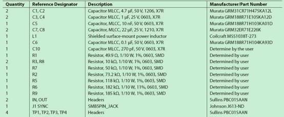
ADP2442设计方案材料清单:
PCB元件布局图:


![]() ADP2441.1.pdf (1.15 MB)
ADP2441.1.pdf (1.15 MB)
![]() ADP2442.2.pdf (332.44 KB)
ADP2442.2.pdf (332.44 KB)
![]() UG-456.1.pdf (325.47 KB)
UG-456.1.pdf (325.47 KB)
![]() UG-456.2.rar (1.84 MB)
UG-456.2.rar (1.84 MB)
责任编辑:David
【免责声明】
1、本文内容、数据、图表等来源于网络引用或其他公开资料,版权归属原作者、原发表出处。若版权所有方对本文的引用持有异议,请联系拍明芯城(marketing@iczoom.com),本方将及时处理。
2、本文的引用仅供读者交流学习使用,不涉及商业目的。
3、本文内容仅代表作者观点,拍明芯城不对内容的准确性、可靠性或完整性提供明示或暗示的保证。读者阅读本文后做出的决定或行为,是基于自主意愿和独立判断做出的,请读者明确相关结果。
4、如需转载本方拥有版权的文章,请联系拍明芯城(marketing@iczoom.com)注明“转载原因”。未经允许私自转载拍明芯城将保留追究其法律责任的权利。
拍明芯城拥有对此声明的最终解释权。
相关资讯
:
基于MC33771主控芯片的新能源锂电池管理系统解决方案

AMIC110 32位Sitara ARM MCU开发方案

基于AMIC110多协议可编程工业通信处理器的32位Sitara ARM MCU开发方案

基于展讯SC9820超低成本LTE芯片平台的儿童智能手表解决方案

基于TI公司的AM437x双照相机参考设计

基于MTK6580芯片的W2智能手表解决方案


 2012- 2022 拍明芯城ICZOOM.com 版权所有 客服热线:400-693-8369 (9:00-18:00)


