


 产品分类
产品分类
Freescale MC9S08MP16马达控制方案
 99
99
 拍明
拍明
原标题:Freescale MC9S08MP16马达控制方案
freescale 公司的MC9S08MP16是低成本8位MCU,用于工业和汽车中夹种速度的马达控制,能提供安全的,精确和低成本的马达控制. MC9S08MP16采用8位HCS08 CPU,2.7V-5.5V和–40℃到125℃温度范围内,CPU速度高达40 MHz,支持48个中断/重置源, 16KB 闪存, 1KB RAM,马达控制专用的1x 2-ch + 1x 6ch FlexTimer,3x高速模拟比较器,可编程增益放大器,2x可编程延迟区块,13路12位2.5us转换时间的ADC.本文介绍了MC9S08MP16主要特性, 方框图和DEMO9S08MP16 评估板详细电路图.
The S08MP16 is a low cost 8-bit MCU that delivers Safe, Accurate and Inexpensive Motor Control for a wide speed range of Industrial and Automotive applications. An ideal entry-level solution for Brushless DC (BLDC) motor applications it features an 8 channel PWM/Flextimer module providing hardware dead-time insertion, Analogue Comparators, Programmable Gain Amplifier, and a 12-bit ADC with PWM hardware triggering. Also offered is an Independently Clocked COP & Cyclic Redundancy Check (CRC) Engine providing clock failure protection & memory content validation for safety-critical applications implementing IEC60730.
MC9S08MP16主要特性:
• 8-Bit HCS08 Central Processor Unit (CPU)
– Up to 51.34 MHz CPU at 2.7V to 5.5V across temperature range of –40°C to 105℃
– Up to 40 MHz CPU at 2.7V to 5.5V across temperature range of –40°C to 125℃
– HC08 instruction set with added BGND instruction and additional addressing modes for LDHX and STHX Support for up to 48 interrupt/reset sources
• On-Chip Memory
– Up to 16 KB flash memory; read/program/erase over full operating voltage and temperature
– Up to 1 KB random-access memory (RAM)
– Security circuitry to prevent unauthorized access to RAM and flash memory contents
• Power-Saving Modes
– Two low power stop modes; reduced power wait mode
– Peripheral clock gating can disable clocks to unused modules
• Clock Source Options
– Oscillator (XOSC) — Loop-control Pierce oscillator; Crystal or ceramic resonator range of 31.25–38.4 kHz or 1–16 MHz
– Internal Clock Source (ICS) — Containing a frequency-locked-loop (FLL) controlled by internal or external reference; precision trimming of internal reference allows 0.2% resolutions and 2% deviation over temperature and voltage; supports CPU frequencies up to 51.34 MHz
• System Protection
– Watchdog computer operating properly (COP) reset running from dedicated 1-kHz internal clock source or bus clock
– Low-voltage detection with reset or interrupt; selectable trip points
– Illegal opcode and illegal address detection with reset
– Flash memory block protection
• Development Support
– Single-wire background debug interface
– Breakpoint capability to allow single breakpoint setting during in-circuit debugging (plus three more breakpoints in on-chip debug module)
– On-chip in-circuit emulator (ICE) debug module containing three comparators and nine trigger modes. Eight deep FIFO for storing change-of-flow addresses and event-only data. Debug module supports both tag and force breakpoints
• Peripherals
– IPC — Interrupt Priority Controller with 4 programmable interrupt priority levels
– ADC—13-channel, 12-bit resolution; 2.5 μs conversion time; automatic compare function; 1.7 mV/℃ temperature sensor; internal bandgap reference channel; operation in stop3
– PGA — Differential programmable gain amplifier with programmable gain (x1, x2, x4, x8, x16, or x32)
– HSCMP — Three fast analog comparators with positive and negative inputs; separately selectable interrupt on rising and falling comparator output; filtering; windowing; HSCMP1 and HSCMP2 outputs can be optionally routed to FTM1 module; runs in stop3
– DAC — Three 5-bit digital to analog convertor used as a 32-tap voltage reference for each comparator
– PDB — Two programmable delay blocks: PDB1 synchronizes PWM with samples of ADC; PDB2 synchronizes PWM with comparing window of analog comparators
– SCI — Full duplex non-return to zero (NRZ); LIN master extended break generation; LIN slave extended break detection; wake up on active edge
– SPI — Full-duplex or single-wire bidirectional; Double-buffered transmit and receive; Master or Slave mode; MSB-first or LSB-first shifting
– IIC/SMBus — Up to 400 kbps; Multi-master operation; Programmable slave address; Interrupt driven byte-by-byte data transfer; supports broadcast mode and 10-bit addressing; SMBus compatible
– FTM — Two Flextimers with total of 8 channels; One 2-channel (FTM1) and one 6-channel (FTM2);supports operation up to 2x bus clock; selectable input capture, output compare, edge- or center-aligned PWM; dead time insertion; fault inputs
– MTIM — 8-bit modulo counter with 8-bit prescaler
– RTC — (Real-time counter) 8-bit modulus counter with binary or decimal based prescaler; External clock source for precise time base, time-of-day, calendar or task scheduling; Free running on-chip low power oscillator (1 kHz) for cyclic wake-up without external components, runs in all MCU modes
– CRC — Cyclic redundancy check generator
– KBI — Three 8 channel keyboard interrupt module with software selectable polarity on edge or edge/level modes
• Input/Output
– 40 GPIOs, 2 output-only pins.
– Hysteresis and configurable pull up device on input pins; Configurable slew rate and drive strength on output pins; Sink/Source current up to 20mA
• Package Options
– 48-LQFP, 32-LQFP, 28-SOIC 48-LQFP qualified for automotive usage
MC9S08MP16目标应用:
Industrial drives/fans/pumps
HVAC systems
Actuator systems
Medical equipment (infusion pumps, respirators, analyzers)
Office Equipment
Small appliance/personal care (food processors, shavers)
Automotive electrical fuel pump
Automotive window lift
Automotive fan control
Automotive high-brightness LEDs
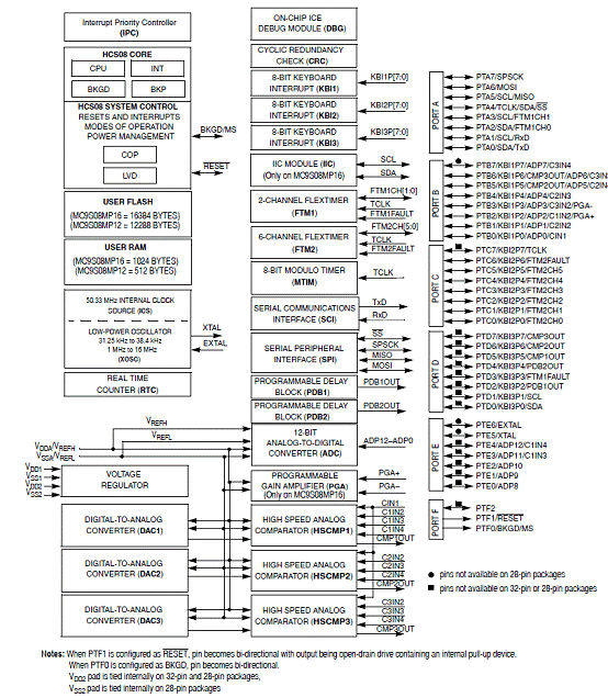
图1.MC9S08MP16系列方框图
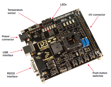
图2.DEMO9S08MP16 评估板外形图
The DEMO9S08MP16 is a cost-effective demo platform for evaluating and developing with the Freescale MC9S08MP16. This low-cost 8-bit MCU is designed to deliver smooth, efficient and safe sensorless BLDC motor control across a wide speed range of industrial and automotive applications.
Peripherals include but are not limited to two 16-bit FlexTimers with deadtime insertion and fault protection in hardware, three high-speed analog comparators, a 6-ch., 16-bit PWM module with emergency over-current shutdown protection, a programmable gain amplifier and a 12-ch., 12-bit ADC with PWM hardware triggering. Also included are an independently clocked COP and cyclic redundancy check (CRC) engine delivering CLK failure protection and memory content validation for safety-critical applications.
责任编辑:David
【免责声明】
1、本文内容、数据、图表等来源于网络引用或其他公开资料,版权归属原作者、原发表出处。若版权所有方对本文的引用持有异议,请联系拍明芯城(marketing@iczoom.com),本方将及时处理。
2、本文的引用仅供读者交流学习使用,不涉及商业目的。
3、本文内容仅代表作者观点,拍明芯城不对内容的准确性、可靠性或完整性提供明示或暗示的保证。读者阅读本文后做出的决定或行为,是基于自主意愿和独立判断做出的,请读者明确相关结果。
4、如需转载本方拥有版权的文章,请联系拍明芯城(marketing@iczoom.com)注明“转载原因”。未经允许私自转载拍明芯城将保留追究其法律责任的权利。
拍明芯城拥有对此声明的最终解释权。
相关资讯
:
基于MC33771主控芯片的新能源锂电池管理系统解决方案

AMIC110 32位Sitara ARM MCU开发方案

基于AMIC110多协议可编程工业通信处理器的32位Sitara ARM MCU开发方案

基于展讯SC9820超低成本LTE芯片平台的儿童智能手表解决方案

基于TI公司的AM437x双照相机参考设计

基于MTK6580芯片的W2智能手表解决方案


 2012- 2022 拍明芯城ICZOOM.com 版权所有 客服热线:400-693-8369 (9:00-18:00)


