


 产品分类
产品分类
Infineon TLE826x系列汽车CAN+LIN收发方案
 238
238
 拍明
拍明
原标题:Infineon TLE826x系列汽车CAN+LIN收发方案
infineon 公司的TLE826x系统基本芯片系列包括TLE8264-2E (3LIN),TLE8263-2E (2LIN),TLE8264E(3LIN), TLE8263E(2LIN),TLE8262E(1LIN)以及TLE8261E (no LIN)等六个产品,主要适合汽车中的CAN-LIN应用如车体控制,网关应用等.芯片包括HS CAN收发器,与ISO 11898-2,11898-5 以及SAE J2284兼容,CAN数据发送速率高达1 MBaud,其中的低压降稳压器,Vcc1μC可提供200mA,5V±2%,Vcc2可提供200mA,5V±2%,而Vcc3可提供400mA,5V±4%.TLE826x系列具有非常低的静态功耗,短路保护和超温保护,采用标准的16位SPI接口.本文介绍TLE826x系列的主要特性,方框图, 功率模式管理方框图, 高速CAN收发器功能方框图, 车体控制器模块应用案例和材料清单(BOM),以及Factor Flash 模式应用建议.
The devices of the SBC family are monolithic integrated circuits in an enhanced power package with identical software functionality and hardware features except for the number of LIN cells. The devices are designed for CAN-LIN automotive applications e.g. body controller, gateway applications.
To support these applications, the System Basis Chip (SBC) provides the main functions, such as HS-CAN transceiver for data transmission, low dropout voltage regulators (LDO) for an external 5 V supply, and a 16-bit Serial Peripheral Interface (SPI) to control and monitor the device. Also implemented are a Time-out or a Window Watchdog circuit with a reset feature, Limp Home circuitry output, and an undervoltage reset feature.The devices offer low power modes in order to support application that are connected permanent to the battery.
A wake-up from the low power mode is possible via a message on the buses or via the bi-level sensitive monitoring/wake-up input as well as from the SPI command. Each wake-up source can be inhibited.
The device is designed to withstand the severe conditions of automotive applications.
scalable System Basis Chip Family
• Six products for complete scalable application coverage
• Complete compatibility (hardware and software) across the family
• TLE8264-2E (3LIN), TLE8263-2E (2LIN) - 3 Limp Home outputs
• TLE8264E (3LIN), TLE8263E (2LIN) - 1 Limp Home output
• TLE8262E (1LIN), TLE8261E (no LIN) - 1 Limp Home output
Basic Features
• Very low quiescent current in Stop and Sleep Modes
• Reset input, output
• Power on and scalable undervoltage reset generator
• Standard 16-bit SPI interface
• Overtemperature and short circuit protection
• Short circuit proof to GND and battery
• One universal wake-up input
• Wide input voltage and temperature range
• Cyclic wake in Stop Mode
• Green Product (RoHS compliant)
• AEC Qualified
HS CAN Transceiver
• Compliant to ISO 11898-2 and 11898-5 as well as SAE J2284
• CAN data transmission rate up to 1 MBaud
• Supplied by dedicated input VccHSCAN
• Low power mode management
• Bus wake-up capability via CAN message
• Excellent EMC performance (very high immunity and very low emission)
• Bus pins are short circuit proof to ground and battery voltage
• 8 kV ESD gun test on CANH / CANL / SPLIT
• Bus failure detection
Voltage Regulators
• Low-dropout voltage regulator
• Vcc1μC, 200 mA, 5 V ±2% for external devices, such as microcontroller and RF receiver
• Vcc2, 200 mA, 5 V ±2% for external devices or the internal HS CAN cell
• Vcc3, current limitation by shunt resistor (up to 400 mA with 220 mΩ shunt resistor), 5 V ±4% with external PNP transistor; for example: to supply additional external CAN transceivers
• Vcc1μC, undervoltage Time-out Supervision
• Reset output with integrated pull-up resistor
• Time-out or Window Watchdog, SPI configured
• Watchdog Timer from 16 ms to 1024 ms
• Check sum bit for Watchdog configuration
• Reset due to Watchdog failure can be inhibited with Test pin (SBC SW Development Mode) Interrupt Management
• Complete enabling / disabling of interrupt sources
• Timing filter mechanism to avoid multiple / infinite Interrupt signals Limp Home
• Open drain Limp Home outputs
• Dedicated internal logic supply
• Maximum safety architecture for Safety Operation Mode
• Configurable Fail-Safe behavior

图1.TLE8261简化方框图
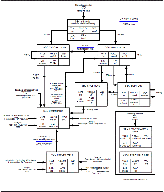
图2.TLE8261功率模式管理方框图
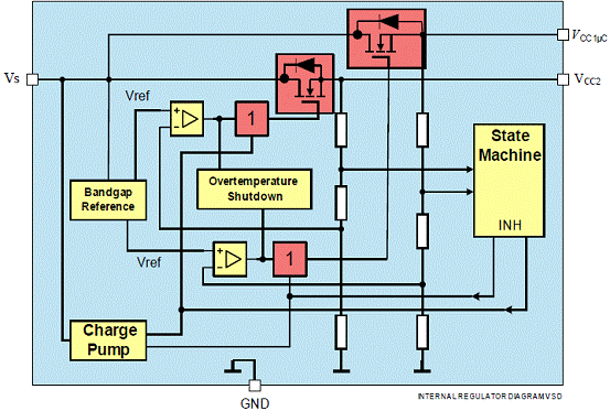
图3.TLE8261内部电压稳压器功能方框图

图4.TLE8261高速CAN收发器功能方框图
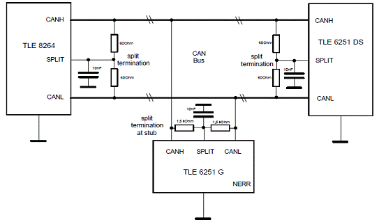
图5.SPLIT引脚应用案例
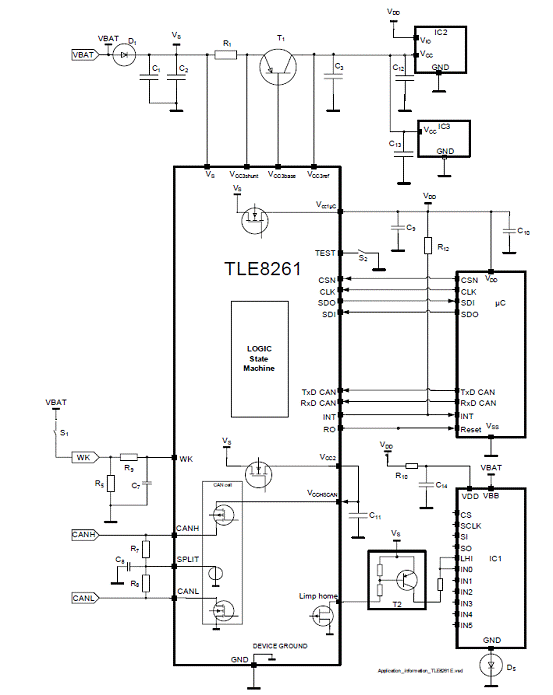
图6.TLE8261车体控制器模块应用案例
应用案例材料清单(BOM):
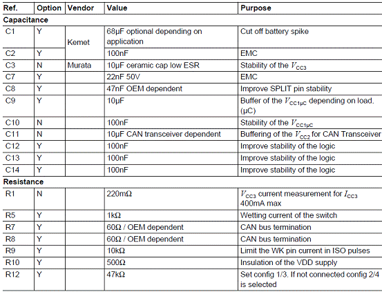
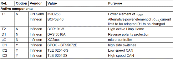
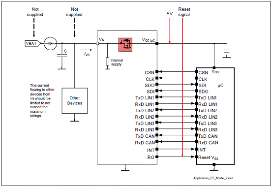
图7. Factor Flash 模式应用建议
责任编辑:David
【免责声明】
1、本文内容、数据、图表等来源于网络引用或其他公开资料,版权归属原作者、原发表出处。若版权所有方对本文的引用持有异议,请联系拍明芯城(marketing@iczoom.com),本方将及时处理。
2、本文的引用仅供读者交流学习使用,不涉及商业目的。
3、本文内容仅代表作者观点,拍明芯城不对内容的准确性、可靠性或完整性提供明示或暗示的保证。读者阅读本文后做出的决定或行为,是基于自主意愿和独立判断做出的,请读者明确相关结果。
4、如需转载本方拥有版权的文章,请联系拍明芯城(marketing@iczoom.com)注明“转载原因”。未经允许私自转载拍明芯城将保留追究其法律责任的权利。
拍明芯城拥有对此声明的最终解释权。
相关资讯
:
基于MC33771主控芯片的新能源锂电池管理系统解决方案

AMIC110 32位Sitara ARM MCU开发方案

基于AMIC110多协议可编程工业通信处理器的32位Sitara ARM MCU开发方案

基于展讯SC9820超低成本LTE芯片平台的儿童智能手表解决方案

基于TI公司的AM437x双照相机参考设计

基于MTK6580芯片的W2智能手表解决方案


 2012- 2022 拍明芯城ICZOOM.com 版权所有 客服热线:400-693-8369 (9:00-18:00)


