


 产品分类
产品分类
Infineon 600 V CoolGaN高压GaN开关绝缘栅驱动方案
 202
202
 拍明
拍明
原标题:Infineon 600 V CoolGaN高压GaN开关绝缘栅驱动方案
infineon公司的600 V CoolGaN高压GaN开关是单路绝缘栅驱动器,是GaN EiceDRIVER™系列产品. CoolGaN™增强模式HEMT是Infineon公司的EiceDRIVER™ IC中1EDF5673K, 1EDF5673F 和1EDS5663H最好驱动器.单路电流绝缘VIO=1500VDC,输出脉冲宽度大于18ns,传输时延精度13ns,降低死区损坏多达50%,可配置和恒定GaN开关转换速率,强健和节能的开关电源(SMPS)设计,缩短产品上市时间,集成的电流绝缘可工作在苛刻的开关应用,可用在需要安全绝缘的地方.本文介绍了CoolGaN HEMT主要特性, 600V CoolGaN大功率SMPS应用案例以及600 V CoolGaN™半桥评估板指标和极限值,应用电路和评估板电路图,材料清单和PCB设计图.
CoolGaN™ e-mode HEMTs are best driven by Infineon’s EiceDRIVER™ ICs, the 1EDF5673K, 1EDF5673F and 1EDS5663H. They ensure robust and highly e_ icient high voltage GaN switch operation whilst concurrently minimizing R&D e_ orts and shortening time-to-market.
CoolGaN HEMT主要特性:
› Low ohmic outputs:
Source: 0.85 _
Sink: 0.35 _
› Single-channel galvanic isolation:
Functional: VIO= 1500 VDC
VIOWM = 510 Vrms (16-pin DSO)
VIOWM = 460 Vrms (LGA 5x5)
Reinforced: VIOTM = 8000 Vpk
(VDE 0884-10 pending)
VIOWM = 1420 VDC
CMTI min: 200 V/ns
› Timing:
Minimum output pulse width: 18 ns
Propagation delay accuracy: 13 ns
Key advantages of designing with the GaN EiceDRIVER™ family
Positive and negative gate drive currents:
› Fast turn-on / turn-o_ GaN switch slew-rates
Firmly hold gate voltage at zero, during o_ -phase:
› Avoids spurious GaN switch turn-on
› Up to 50% lower dead-time losses
Configurable and constant GaN switching slew-rates, across wide range of switching
frequency and duty-cycle:
› Robust and energy e_ icient SMPS designs
› Short time-to-market
Integrated galvanic isolation:
› Robust operation in hard-switching applications
› Safe isolation where needed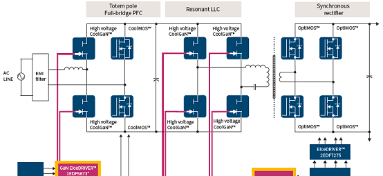
图1. 600V CoolGaN大功率SMPS应用案例
600 V CoolGaN™半桥评估板
600 V CoolGaN™ half-bridge evaluation platform featuring GaN EiceDRIVER™
600 V CoolGaN™ half-bridge evaluation platform
This 600 V Gallium Nitride (GaN) half-bridge evaluation board enables easy, rapid setup and test of CoolGaN™ transistors along with the dedicated GaN EiceDRIVER™ isolated gate driver IC. The generic topology is configurable for boost or buck operation, pulse testing or continuous full-power operation. Test points provide easy access to connect signals to an oscilloscope for measuring the switching performance of CoolGaN™ transistors and gate driver. This board saves the user the time to design their own gate driver and power circuit to evaluate GaN power transistors.
The half-bridge circuit board has a single PWM input intended for connection to a 50 Ω pulse or signal generator. Board power comes from a single 5 V supply input, which powers everything including the isolated gate driver power supplies. Deadtime between the high and low-side is pre-set to 100 ns, but is adjustable via trimpots. An external (user-supplied) inductor connects to the supplied pluggable terminal-block connector. The output and bus voltage can range up to 450 V, limited by the capacitor rating. This half-bridge can switch continuous currents of 12 A, and peak currents of 35 A, hard or soft-switching. Operating frequency can be up to several MHz, depending on transistor dissipation (limited to about 15 W per device with appropriate heatsink and airflow).
This Application Note explains how to set-up and use the 600 V CoolGaN™ half-bridge evaluation board. The board features a half-bridge of 70 mΩ GaN power transistors, and a pair of EiceDRIVER™ GaN gate drivers, along with input logic that provides adjustable deadtime. Using an external inductor, the board can be configured for buck or boost-mode, double-pulse testing or continuous PWM operation, hard or soft-switching at power levels to several kW and frequencies into the MHz.
This document is intended for power electronic engineers and designers who are already familiar with MOSFET or IGBT-based converters, inverters and gate drivers, who are interested in looking at the similarities and differences of GaN power transistors compared to their Silicon counterparts.
600 V CoolGaN™半桥评估板指标和极限值: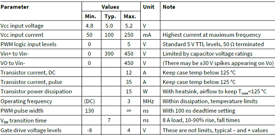

图2. 600 V CoolGaN™半桥评估板前和后外形图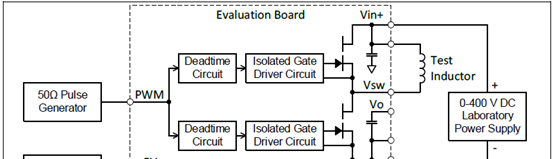
图3.600 V CoolGaN™半桥评估板应用案例(双脉冲测试)
图4.600 V CoolGaN™半桥评估板反向双脉冲测试图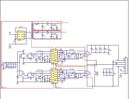
图5.600 V CoolGaN™半桥评估板电路图
600 V CoolGaN™半桥评估板材料清单:

图6. CoolGaN™半桥评估板PCB设计图:顶层铜和元件布局图
图7. CoolGaN™半桥评估板PCB设计图:上中层铜布局图和底层元件套图
图8. CoolGaN™半桥评估板PCB设计图:下中层铜布局图和底层元件套图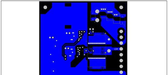
图9. CoolGaN™半桥评估板PCB设计图:底层铜布局图和底层元件套图(从顶层看)
责任编辑:
【免责声明】
1、本文内容、数据、图表等来源于网络引用或其他公开资料,版权归属原作者、原发表出处。若版权所有方对本文的引用持有异议,请联系拍明芯城(marketing@iczoom.com),本方将及时处理。
2、本文的引用仅供读者交流学习使用,不涉及商业目的。
3、本文内容仅代表作者观点,拍明芯城不对内容的准确性、可靠性或完整性提供明示或暗示的保证。读者阅读本文后做出的决定或行为,是基于自主意愿和独立判断做出的,请读者明确相关结果。
4、如需转载本方拥有版权的文章,请联系拍明芯城(marketing@iczoom.com)注明“转载原因”。未经允许私自转载拍明芯城将保留追究其法律责任的权利。
拍明芯城拥有对此声明的最终解释权。
相关资讯
:
基于MC33771主控芯片的新能源锂电池管理系统解决方案

AMIC110 32位Sitara ARM MCU开发方案

基于AMIC110多协议可编程工业通信处理器的32位Sitara ARM MCU开发方案

基于展讯SC9820超低成本LTE芯片平台的儿童智能手表解决方案

基于TI公司的AM437x双照相机参考设计

基于MTK6580芯片的W2智能手表解决方案


 2012- 2022 拍明芯城ICZOOM.com 版权所有 客服热线:400-693-8369 (9:00-18:00)


