


 产品分类
产品分类
Freescale Flexis QE128血压计解决方案
 95
95
 拍明
拍明
原标题:Freescale Flexis QE128血压计解决方案
freescale 公司的Flexis QE128是采用8位HCS08 CPU的微控制器,2.4V时的工作频率高达50.33MHz,2.1V时为40MHz,而1.8V时为20MHz,具有128KB 闪存,25个ADC通路,提供高达25MHz的总线频率.支持多达32个中断/重置源.血压计(BPM)参考设计采用Freescale公司的Flexis MC9S08QE128 MCU, Flexis MCF51QE128, MPR083接近式传感器, MR2A16A异步磁阻RAM, MC9S08JM60 微控制器, MC13202 ZigBee收发器, PXV5050压力传感器和OSRAM 公司的Pictiva OLED 显示器OS128064PK27MY0B00M.本文介绍了Flexis QE128的主要特性和方框图,血压计(BPM)参考设计的主要优势,方框图以及详细的电路图和所用材料清单(BOM).
MC9S08QE128 Series comprised of a pin-compatible 8-bit and 32-bit device duo, is the first family in the Flexis series. The FlexisTM series of controllers is the connection point of the Freescale Controller Continuum, where 8- and 32-bit compatibility becomes reality, delivering the ultimate in migration flexibility.
The S08QE128 pushes the boundaries of the 8-bit architecture performance with 128Kb of Flash, 24 ADC channels and delivering up 25MHz in bus frequency. The 32-bit MCF51QE128 is pin-, peripheral- and tool-compatible with the 8-bit S08QE128 device. They share a common set of peripherals and development tools delivering the ultimate in migration flexibility.
主要特性:
8-Bit HCS08 Central Processor Unit (CPU)
Up to 50.33-MHz HCS08 CPU above 2.4V, 40-MHz CPU above 2.1V, and 20-MHz CPU above 1.8V, across temperature range
HC08 instruction set with added BGND instruction
Support for up to 32 interrupt/reset sources
On-Chip Memory
Flash read/program/erase over full operating voltage and temperature
Random-access memory (RAM)
Security circuitry to prevent unauthorized access to RAM and flash contents
Power-Saving Modes
Two low power stop modes; reduced power wait mode
Peripheral clock enable register can disable clocks to unused modules, reducing currents; allows clocks to remain enabled to specific peripherals in stop3 mode
Very low power external oscillator can be used in stop3 mode to provide accurate clock to active peripherals
Very low power real time counter for use in run, wait, and stop modes with internal and external clock sources
6 μs typical wake up time from stop modes
Clock Source Options
Oscillator (XOSC) — Loop-control Pierce oscillator; Crystal or ceramic resonator range of 31.25 kHz to 38.4 kHz or 1 MHz to 16 MHz
Internal Clock Source (ICS) — FLL controlled by internal or external reference; precision trimming of internal reference allows 0.2% resolution and 2% deviation; supports CPU freq. from 2 to 50.33 MHz
System Protection
Watchdog computer operating properly (COP) reset with option to run from dedicated 1-kHz internal clock source or bus clock
Low-voltage detection with reset or interrupt; selectable trip points
Illegal opcode detection with reset
Flash block protection
Development Support
Single-wire background debug interface
Breakpoint capability to allow single breakpoint setting during in-circuit debugging (plus two more breakpoints)
On-chip in-circuit emulator (ICE) debug module containing two comparators and nine trigger modes. Eight deep FIFO for storing change-of-flow addresses and event-only data. Debug module supports both tag and force breakpoints.
ADC — 24-channel, 12-bit resolution; 2.5 μs conversion time; automatic compare function; 1.7 mV/℃ temperature sensor; internal bandgap reference channel; operation in
stop3; fully functional from 3.6V to 1.8V
ACMPx — Two analog comparators with selectable interrupt on rising, falling, or either edge of comparator output; compare option to fixed internal bandgap reference voltage; outputs can be optionally routed to TPM module; operation in stop3
SCIx — Two SCIs with full duplex non-return to zero (NRZ); LIN master extended break generation; LIN slave extended break detection; wake up on active edge
SPIx— Two serial peripheral interfaces with Full-duplex or single-wire bidirectional; Double-buffered transmit and receive; MSB-first or LSB-first shifting
IICx — Two IICs with; Up to 100 kbps with maximum bus loading; Multi-master operation; Programmable slave address; Interrupt driven byte-by-byte data transfer; supports broadcast mode and 10 bit addressing
TPMx — One 6-channel and two 3-channel; Selectable input capture, output compare, or buffered edge- or center-aligned PWMs on each channel
RTC — 8-bit modulus counter with binary or decimal based prescaler; External clock source for precise time base, time-of-day, calendar or task scheduling functions; Free running on-chip low power oscillator (1 kHz) for cyclic wake-up without external components
Input/Output
70 GPIOs and 1 input-only and 1 output-only pin
16 KBI interrupts with selectable polarity
Hysteresis and configurable pull-up device on all input pins; Configurable slew rate and drive strength on all output pins.
SET/CLR registers on 16 pins (PTC and PTE)
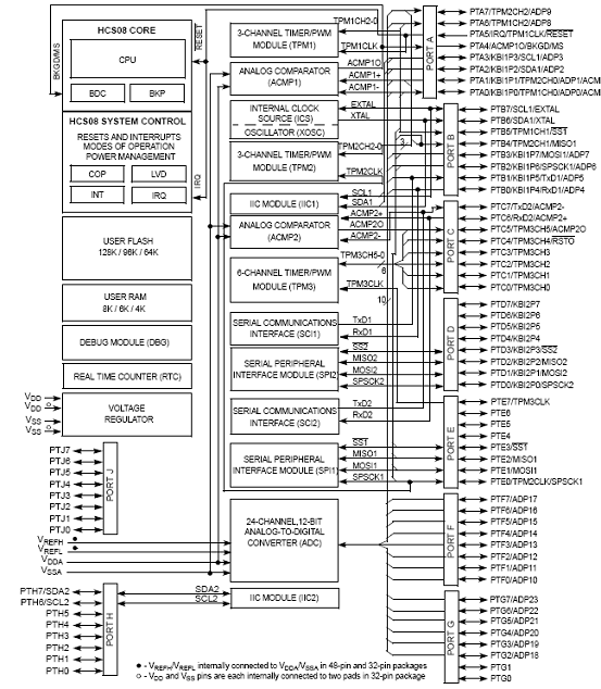
图1.MC9S08QE128系列方框图
血压计(BPM)参考设计
The blood pressure monitor (BPM) reference design shows how to implement a system that can measure arterial blood pressure values. The system demonstrates control, data retention, analog acquisition, and connectivity functions, as well as the ability to interface with a user. These are achieved by using several Freescale devices.
This reference design serves only as a proof of concept for this application and is not authorized for use in safety-critical applications such as a U.S. Food and Drug Administration (FDA) class 3 application.
Manufacturers and designers who incorporate Freescale (FSL) technology must have all necessary expertise in the safety and regulatory ramifications involved in the application of this design, and they are solely responsible for all legal, regulatory, and safety-related requirements concerning their products and the use of Freescale devices in safety-critical applications.
解决方案优势:
The BPM reference design elements can be referenced for later development as:
USB communication using the MC9S08JM60 as a bridge
2.4 GHz communication using the MC13202 ZigBee transceiver
MRAM communications
Use of MRAM to store user data
MRAM driver to access MRAM memory
User display using an OLED display
User interface using the MPR083 proximity sensor
Audio feedback using two timer pulse-width modulator (TPM) modules
The main benefit from this solution is that developers are able to take any piece of hardware and/or software and reuse it for their own applications, thus enhancing the design cycle and providing faster development time.
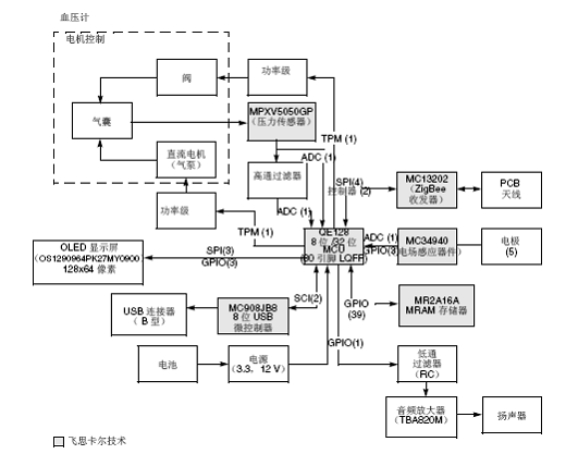
图2. Flexis QE128 血压计(BPM)参考设计方框图
The design for the BPM PCB was made with the intention of isolating the different blocks of the system to avoid letting coupling noise into the lines of the instrumentation amplifier. The power is segmented through the use of 0 Ω resistors for debugging. These resistors can be replaced by ferrite cores to suppress EMI and noise coming from the different portions of the board. Ground distribution was implemented using a star configuration.
Another feature of the board is the test socket which eases the change between the S08 and the ColdFire device.
This section provides the technical descriptions for the Freescale BPM system, and for the Freescale components used in the reference design. These Freescale components are:
Flexis MC9S08QE128 Microcontroller
Flexis MCF51QE128 Microcontroller
MPR083 Proximity Sensor
MR2A16A Asynchronous Magnetoresistive RAM
MC9S08JM60 Microcontroller
MC13202 ZigBee Transceiver
MPXV5050 Pressure Sensor
OSRAM Pictiva OLED Display OS128064PK27MY0B00
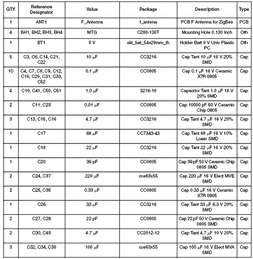
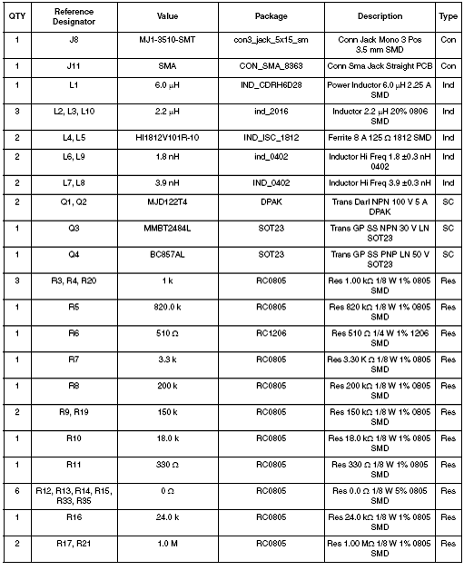
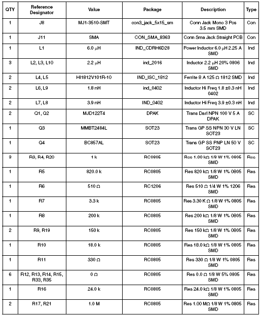
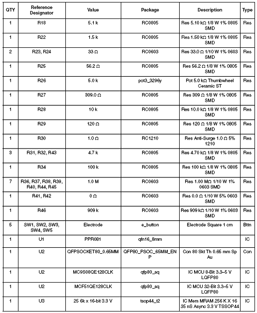
Flexis QE128 血压计(BPM)参考设计材料清单(BOM):

责任编辑:David
【免责声明】
1、本文内容、数据、图表等来源于网络引用或其他公开资料,版权归属原作者、原发表出处。若版权所有方对本文的引用持有异议,请联系拍明芯城(marketing@iczoom.com),本方将及时处理。
2、本文的引用仅供读者交流学习使用,不涉及商业目的。
3、本文内容仅代表作者观点,拍明芯城不对内容的准确性、可靠性或完整性提供明示或暗示的保证。读者阅读本文后做出的决定或行为,是基于自主意愿和独立判断做出的,请读者明确相关结果。
4、如需转载本方拥有版权的文章,请联系拍明芯城(marketing@iczoom.com)注明“转载原因”。未经允许私自转载拍明芯城将保留追究其法律责任的权利。
拍明芯城拥有对此声明的最终解释权。
相关资讯
:
基于MC33771主控芯片的新能源锂电池管理系统解决方案

AMIC110 32位Sitara ARM MCU开发方案

基于AMIC110多协议可编程工业通信处理器的32位Sitara ARM MCU开发方案

基于展讯SC9820超低成本LTE芯片平台的儿童智能手表解决方案

基于TI公司的AM437x双照相机参考设计

基于MTK6580芯片的W2智能手表解决方案


 2012- 2022 拍明芯城ICZOOM.com 版权所有 客服热线:400-693-8369 (9:00-18:00)


