


 产品分类
产品分类
TI TIDA-010039三相SiC AC-DC转换器参考设计
 286
286
 拍明
拍明
原标题:TI TIDA-010039三相SiC AC-DC转换器参考设计
TI公司的TIDA-010039是三级三相SiC AC/DC转换器参考设计,提供了如何实现具有双向功能的三级三相基于SiC的AC/DC转换器.其高开关频率50kHz降低滤波器设计中的磁性元件尺寸,从而获得更高的功率密度. SiC MOSFET具有低开关损耗,使得更高的DC总线电压高达800V,较低开关损耗具有峰值效率大于97%.参考设计的输入为380–400 VAC峰值,DC输出为800V,在400-VAC 50或60-Hz电网连接时,最大输出功率为10-kW, 10-kVA,隔离驱动器ISO5852S具有增强的绝缘性能,用来驱动高压SiC MOSFET,而UCC5320S则用来驱动中等Si IGBT.采用AMC1301来监测负载电流,而TMS320F28379D控制卡用来数字控制.主要用在DC充电桩,电动汽车充电站功率模块,能量存储转换系统(PCS)和三相UPS.本文介绍了三相SiC AC/DC转换器参考设计TIDA-010039主要特性,框图和主要系统指标,以及电路图.
This reference design provides an overview on how to implement a three-level, three-phase, SiC-based AC/DC converter with bidirectional functionality. A high switching frequency of 50 kHz reduces the size of magnetics for the filter design and as a result a higher power density. SiC MOSFETs with low switching loss enable higher DC bus voltages of up to 800 V and lower switching losses with a peak efficiency of > 97%.
This design is configurable to work as a two-level or three-level rectifier. For design information on theDC/AC implementation, see TIDA-01606.
Newer generations of Electric Vehicles (EVs) are pushing the battery capacity and charging rates higher and higher to meet consumer demand for longer range and less time spent with the vehicle plugged in. To support these new trends, EV charging stations need to supply more power than ever before.
In addition to higher power levels, additional trends in the EV charging market are pushing the technology in other fronts:
1. Higher voltage batteries
2. Bidirectional power flow
3. Increased power density
By increasing battery voltage, more power to the vehicle can be realized at the same current levels. This also maintains or reduces the amount of copper and results in smaller power devices required in the power stages of the charging station. The reduction in di/dt also reduces the stress on electrical components. However, sustained DC voltages of > 800 V can be difficult to design to, or even find components that can survive it, especially in high switch frequency designs.
Bidirectional power flow from the grid to the battery, and battery to grid, is enabling the battery of the vehicle to serve as a distributed energy resource. This allows for grid load balancing when renewable resources are low, or to accommodate demand shift throughout the day.
To compensate for the voltage stresses generated by high-voltage batteries, and enable bidirectional power flow, new topologies of converters have been designed. Traditional half bridges block the full input voltage on each switching device. By adding additional switched blocking and conduction components, the overall stress on the device can be significantly reduced. This reference design shows how to implement a three-level converter. Higher level converters are also possible, further increasing the voltage handling capability.
Additional power density in power electronics is also being enabled by moving to higher switching speeds in the power converters. As this design shows, even a modestly higher switching speed reduces the overall size requirement of the output filter stage—a primary contributor to the design size.
Traditional switching devices have a limit in how quickly they can switch high voltages, or more appropriately, the dV/dt ability of the device. This slow ramp up and down increases switching loss because the device spends more time in a switching state. This increased switch time also increases the amount of dead time required in the control system to prevent shoot-through and shorts. The solution to this has been developed in newer switching semiconductor technology like SiC and GaN devices with high electron mobility. This reference design uses SiC MOSFETs alongside TI’s SiC gate driver technology to
demonstrate the potential increase in power density.
三相SiC AC/DC转换器参考设计TIDA-010039主要特性:
• Rated nominal input of 380–400 VAC peak, with DC output of 800 V
• Maximum 10-kW, 10-kVA output power at 400-VAC 50- or 60-Hz grid connection
• High-voltage (1200 V) SiC MOSFET-based fullbridge AC/DC converter for peak efficiency of > 97%
• Compact filter by switching rectifier at 50 kHz
• Isolated driver ISO5852S with reinforced isolation for driving high-voltage SiC MOSFET and UCC5320S for driving middle Si IGBT
• Isolated current sensing using the AMC1301 for load current monitoring
• TMS320F28379D control card for digital control
参考设计TIDA-010039应用:
• DC Charging (Pile) Station
• EV Charging Station Power Module
• Energy Storage Power Conversion System (PCS)
• Three Phase UPS
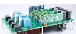
图1. 参考设计TIDA-010039外形图
TIDA-010039 Three-level, three-phase SiC AC-to-DC converter reference design board image
参考设计TIDA-010039主要系统指标:
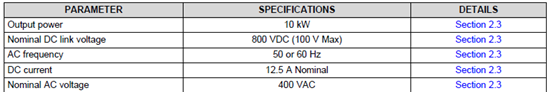
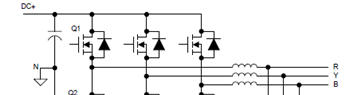
图3. 两级三相转换器架构图
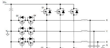
图4. 三级T型三相转换器架构图
责任编辑:David
【免责声明】
1、本文内容、数据、图表等来源于网络引用或其他公开资料,版权归属原作者、原发表出处。若版权所有方对本文的引用持有异议,请联系拍明芯城(marketing@iczoom.com),本方将及时处理。
2、本文的引用仅供读者交流学习使用,不涉及商业目的。
3、本文内容仅代表作者观点,拍明芯城不对内容的准确性、可靠性或完整性提供明示或暗示的保证。读者阅读本文后做出的决定或行为,是基于自主意愿和独立判断做出的,请读者明确相关结果。
4、如需转载本方拥有版权的文章,请联系拍明芯城(marketing@iczoom.com)注明“转载原因”。未经允许私自转载拍明芯城将保留追究其法律责任的权利。
拍明芯城拥有对此声明的最终解释权。
相关资讯
:
基于MC33771主控芯片的新能源锂电池管理系统解决方案

AMIC110 32位Sitara ARM MCU开发方案

基于AMIC110多协议可编程工业通信处理器的32位Sitara ARM MCU开发方案

基于展讯SC9820超低成本LTE芯片平台的儿童智能手表解决方案

基于TI公司的AM437x双照相机参考设计

基于MTK6580芯片的W2智能手表解决方案


 2012- 2022 拍明芯城ICZOOM.com 版权所有 客服热线:400-693-8369 (9:00-18:00)


