ST STPMIC1低功耗微处理器功率管理解决方案
 118
118
 拍明
拍明
原标题:ST STPMIC1低功耗微处理器功率管理解决方案
ST公司的 STPMIC1是用于微处理器单元的高度集成功率管理集成电路,具有先进的低功耗特性,由主处理器通过I²C和IO接口来控制.STPMIC1稳压器设计用来给应用处理器和外接系统外设如DDR,闪存和其它系统设备等供电.升压转换器能给多达3个USB端口(两个500mA主USB和100mA USB OTG)供电.输入电压范围从2.8V到5.5V,有4路可调整的通用LDO,1个LDO用于DDR3终端(沉-源),旁路模式用于低功耗DDR或通用LDO.1个LDO用于USB PHY电源和自动电源检测.1个基准电压LDO用于DDR存储器.4个自适应恒定时间(COT)降压SMPS转换器,带旁路模式的5.2V/1.1A升压SMPS用于5V输入或电池输入,1个和500 mA USB OTG兼容的功率开关.主要用在嵌入微处理器单元的电源管理,可穿戴和IoT,手持设备,人机接口,智能家居等.本文介绍了STPMIC1主要特性,典型应用电路和评估板STEVAL-PMIC1K1主要特性,电路图,材料清单和PCB设计图.
The STPMIC1 is a fully integrated power management IC designed for productsbased on high integrated application processor designs requiring low power and highefficiency.
The device integrates advanced low power features controlled by a host processorvia I²C and IO interface.
The STPMIC1 regulators are designed to supply power to the application processoras well as to the external system peripherals such as: DDR, Flash memories andother system devices.
The boost converter can power up to 3 USB ports (two 500 mA host USB and one100 mA USB OTG). Its advanced bypass architecture allows the smooth regulationof VBUS for USB ports from a battery as well as low-cost consumer 5 V AC-DCadapters.
4 buck SMPS are optimized to provide an excellent transient response and an outputvoltage precision for a wide range of operating conditions, high full range efficiency (ηup to 90%) by implementing a low power mode with a smooth transition from PFM toPWM and also an advanced PWM synchronization technique with an integrated PLLfor a better noise (EMI performance).
STPMIC1主要特性:
• Input voltage range from 2.8 V to 5.5 V
• 4 adjustable general purpose LDOs
• 1 LDO for DDR3 termination (sink-source), bypass mode for low power DDR oras general purpose LDO
• 1 LDO for USB PHY supply with automatic power source detection
• 1 reference voltage LDO for DDR memory
• 4 adjustable adaptive constant on-time (COT) buck SMPS converters
• 5.2 V / 1.1 A boost SMPS with bypass mode for 5 V input or battery input
• 1 power switch 500 mA USB OTG compliant
• 1 power switch 500 mA/1000 mA general purpose
• User programmable non-volatile memory (NVM), enabling scalability to supporta wide range of applications
• I²C and digital IO control interface
• WFQFN 44L (5x6x0.8)
STPMIC1应用:
• Power management for embedded micro processor units
• Wearable and IoT
• Portable devices
• Man-machine interfaces
• Smart home
• Power management unit companion chip of the STM32MP1 MPU
The STPMIC1 has a non-volatile memory (NVM) that enables scalability to support a wide range of applications:
• Default output voltage, POWER_UP/POWER_DOWN sequence, protection behavior, auto turn-onfunctionality, I2C slave address
• The STPMIC1A and STPMIC1B are pre-programmed devices to support the STM32MP1 series applicationprocessor versions
• The STPMIC1C is not a programmed device to support custom applications
• Straightforward NVM (re)programming via I2C to facilitate mass production directly in target applications
• Possibility to lock NVM content to prevent further re-programming by writing LOCK_NVM bit

图1.STPMIC1典型应用电路
评估板STEVAL-PMIC1K1
The STEVAL-PMIC1K1 evaluation board is designed for testing and evaluation of the STPMIC1 power management IC forapplication processors requiring low power and high efficiency. The STPMIC1 integrates a range of regulators, converters, andswitches to manage the power requirements of STM32MP1 series microprocessors as well as other application processors andperipherals such as DDR, Flash, USB and other system devices.
The evaluation board is highly configurable and can be programmed via I²C to suit many power supply requirements of MPUbasedapplications such as IoT, human machine interfaces, Smart Home, etc.
The 6.1x7.2cm evaluation board is provided with 2.54mm header for each regulators output, some jumpers are present on theboard for fast and easy setup accordingly to the application needs. For each output a TP is present for sensing the outputvoltage. User management buttons, Reset, Wakeup and Ponkey, are available for easy work. Dedicated connectors for digitalsection are present for I/O and I²C communication up to 1Mb/s

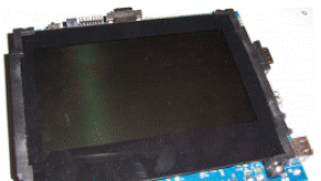
图2.评估板STEVAL-PMIC1K1外形图

图3.评估板STEVAL-PMIC1K1电路图

图4.评估板STEVAL-PMIC1K1电源管理IC电路图
评估板STEVAL-PMIC1K1材料清单:


责任编辑:David
【免责声明】
1、本文内容、数据、图表等来源于网络引用或其他公开资料,版权归属原作者、原发表出处。若版权所有方对本文的引用持有异议,请联系拍明芯城(marketing@iczoom.com),本方将及时处理。
2、本文的引用仅供读者交流学习使用,不涉及商业目的。
3、本文内容仅代表作者观点,拍明芯城不对内容的准确性、可靠性或完整性提供明示或暗示的保证。读者阅读本文后做出的决定或行为,是基于自主意愿和独立判断做出的,请读者明确相关结果。
4、如需转载本方拥有版权的文章,请联系拍明芯城(marketing@iczoom.com)注明“转载原因”。未经允许私自转载拍明芯城将保留追究其法律责任的权利。
拍明芯城拥有对此声明的最终解释权。


 产品分类
产品分类




 2012- 2022 拍明芯城ICZOOM.com 版权所有 客服热线:400-693-8369 (9:00-18:00)


