


 产品分类
产品分类
Renesas RL78/G14系列低功耗高性能MCU解决方案
 224
224
 拍明
拍明
原标题:Renesas RL78/G14系列低功耗高性能MCU解决方案
Renesas公司的RL78/G14系列是低功耗高性能通用微控制器(mcu),CPU最低功耗为66 μA/MHz,待机(停止)为240 nA;高计算功能为 51.2 DMIPS (32 MHz).内置的高功能计时器采用三相互补PWM输出,支持三相马达控制.MCU具有片上振荡器,数据闪存,ADC和DAC,比较器等.内置的安全特性支持家用电器安全(IEC/UL 60730).器件具有30引脚到100引脚,高达512KB闪存,使得器件有广泛的应用如马达控制,消费类电子和工业设备.RL78/G14系列真正的低功耗平台(低到66 μA/MHz和RTC+LVD 的0.60 μA ),1.6V-5.5V工作,16-512KB闪存,32MHz时的DMIPS为44,很适合于通用应用.本文介绍了RL78/G14系列主要特性,30引脚到100引脚器件框图,以及RL78/G14系列原型板主要特性和指标,框图,运行图,以及电路图,材料清单和PCB元件布局图.
RL78/G14 microcontrollers balance the industry’s lowest level of consumption current (CPU: 66 μA/MHz, standby (STOP): 240 nA) and a high calculation performance of 51.2 DMIPS (32 MHz). The built-in high-function timer supports three-phase motor control using three-phase complementary PWM output. They have an on-chip oscillator, data flash, A/D and D/A converters, comparator, and more. Built-in safety features (function that detects illegal operation of hardware) enable support for the household appliance safety standard (IEC/UL 60730). With a broad 30 to 100-pin lineup and up to 512 KB on-chip flash memory, these microcontrollers can be used in a wide variety of applications such as motor control and consumer and industrial equipment.
True Low Power Platform (as low as 66 μA/MHz, and 0.60 μA for RTC + LVD), 1.6 V to 5.5 V operation,16 to 512 Kbyte Flash, 44 DMIPS at 32 MHz, for General Purpose Applications.
RL78/G14系列主要特性:
Ultra-Low Power Consumption Technology
• VDD = single power supply voltage of 1.6 to 5.5 V whichcan operate a 1.8 V device at a low voltage
• HALT mode
• STOP mode
• SNOOZE mode
RL78 CPU Core
• CISC architecture with 3-stage pipeline
• Minimum instruction execution time: Can be changedfrom high speed (0.03125 μs: @ 32 MHz operation withhigh-speed on-chip oscillator) to ultra-low speed (30.5μs: @ 32.768 kHz operation with subsystem clock)
• Multiply/divide/multiply & accumulate instructions aresupported.
• Address space: 1 MB
• General-purpose registers: (8-bit register × 8) × 4 banks
• On-chip RAM: 2.5 to 48 KB
Code Flash Memory
• Code flash memory: 16 to 512 KB
• Block size: 1 KB
• Prohibition of block erase and rewriting (securityfunction)
• On-chip debug function
• Self-programming (with boot swap function/flash shieldwindow function)
Data Flash Memory
• Data flash memory: 4 KB and 8 KB
• Back ground operation (BGO): Instructions can beexecuted from the program memory while rewriting thedata flash memory.
• Number of rewrites: 1,000,000 times (TYP.)
• Voltage of rewrites: VDD = 1.8 to 5.5 V
High-speed On-chip Oscillator
• Select from 64 MHz, 48 MHz, 32 MHz, 24 MHz, 16 MHz,
12 MHz, 8 MHz, 6 MHz, 4 MHz, 3 MHz, 2 MHz, and1 MHz
• High accuracy: ±1.0% (VDD = 1.8 to 5.5 V, TA = -20 to+85℃
Operating Ambient Temperature
• TA = -40 to +85℃ (A: Consumer applications, D:Industrial applications)
• TA = -40 to +105℃ (G: Industrial applications)
Power Management and Reset Function
• On-chip power-on-reset (POR) circuit
• On-chip voltage detector (LVD) (Select interrupt andreset from 14 levels)
Data Transfer Controller (DTC)
• Transfer modes: Normal transfer mode, repeat transfermode, block transfer mode
• Activation sources: Activated by interrupt sources.
• Chain transfer function
Event Link Controller (ELC)
• Event signals of 19 to 26 types can be linked to thespecified peripheral function.
Serial Interfaces
• CSI: 3 to 8 channels
• UART/UART (LIN-bus supported): 3 or 4 channels
• I2C/simplified I2C: 3 to 8 channels
Timer
• 16-bit timer: 8 to 12 channels
(Timer Array Unit (TAU): 4 to 8 channels, Timer RJ: 1channel, Timer RD: 2 channels, Timer RG: 1 channel)
• 12-bit interval timer: 1 channel
• Real-time clock: 1 channel (calendar for 99 years, alarmfunction, and clock correction function)
• Watchdog timer: 1 channel (operable with the dedicatedlow-speed on-chip oscillator)
A/D Converter
• 8/10-bit resolution A/D converter (VDD = 1.6 to 5.5 V)
• Analog input: 8 to 20 channels
• Internal reference voltage (1.45 V) and temperaturesensor
D/A Converter
• 8-bit resolution D/A converter (VDD = 1.6 to 5.5 V)
• Analog output: None or up to two channels
• Output voltage: 0 V to VDD
• Real-time output function
Comparator
• None or up to two channels
• Operating modes: Comparator high-speed mode,comparator low-speed mode, window mode
• The external reference voltage or internal referencevoltage can be selected as the reference voltage.
I/O Port
• I/O port: 26 to 92 (N-ch open drain I/O [withstandvoltage of 6 V]: 2 to 4, N-ch open drain I/O [VDDwithstand voltage/EVDD withstand voltage]: 10 to 28)
• Can be set to N-ch open drain, TTL input buffer, and onchippull-up resistor
• Different potential interface: Can connect to a 1.8/2.5/3V device
• On-chip key interrupt function
• On-chip clock output/buzzer output controller
Others
• On-chip BCD (binary-coded decimal) correction circuit

图1.30引脚RL78/G14系列框图
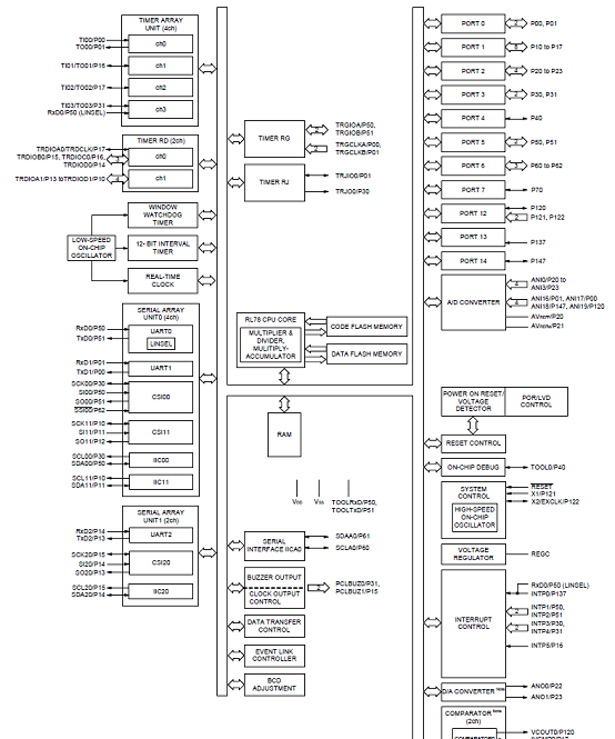
图2.32引脚RL78/G14系列框图
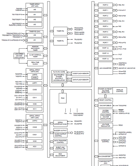
图3. 36引脚RL78/G14系列框图

图4. 40引脚RL78/G14系列框图
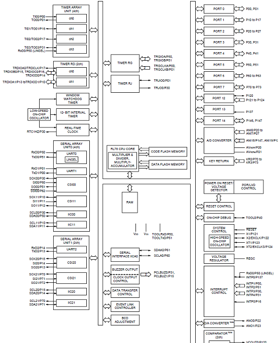
图5. 44引脚RL78/G14系列框图
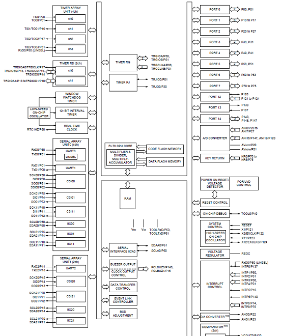
图6. 48引脚RL78/G14系列框图
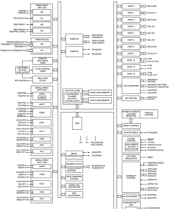
图7. 52引脚RL78/G14系列框图

图8. 64引脚RL78/G14系列框图
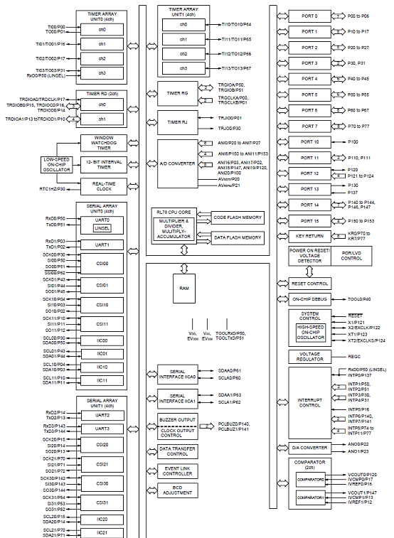
图9. 80引脚RL78/G14系列框图
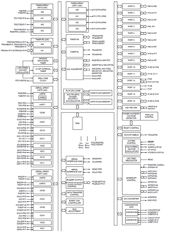
图10. 100引脚RL78/G14系列框图
RL78/G14系列原型板
The RL78/G14 Fast Prototyping Board comes equipped with a high-performance RL78/G14 microcontroller and is an evaluation board specialized for prototype development for a variety of applications. It has a built-in emulator circuit that is equivalent to an E2 emulator Lite so you can write/debug programs without additional tools. In addition, with Arduino Uno and Pmod™ interfaces included standard and through-hole access to all pins of the microcontroller, and so on, it has high scalability.
It is also possible to prototype IoT sensor devices using wireless communication based on LoRa® by combining with a Semtech SX1261/SX1262 LoRa® transceiver.
RL78/G14系列原型板主要特性:
Equipped with an RL78/G14 16-bit microcontroller (80-pin, ROM: 512KB, RAM: 48KB)
No additional tools are required for program debugging/writing with the built-in emulator circuit equivalent to an E2 emulator Lite
Through-holes with access to all of the pins of the microcontroller
Arduino Uno and Pmod™ interfaces come standard
Support for various RL78 software and tools
RL78/G14系列原型板主要指标:

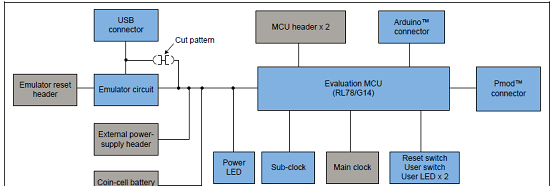
图11. RL78/G14系列原型板框图
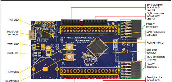
图. RL78/G14系列原型板布局图(顶层)

图. RL78/G14系列原型板运行环境图

图15. RL78/G14系列原型板电路图(1)

图. RL78/G14系列原型板电路图(2)
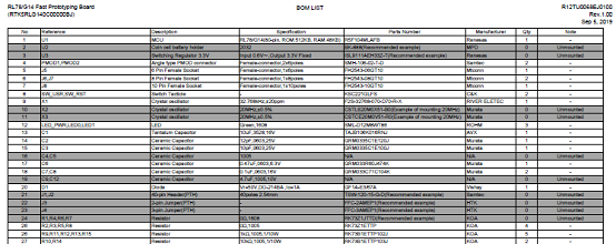
RL78/G14系列原型板材料清单:
责任编辑:David
【免责声明】
1、本文内容、数据、图表等来源于网络引用或其他公开资料,版权归属原作者、原发表出处。若版权所有方对本文的引用持有异议,请联系拍明芯城(marketing@iczoom.com),本方将及时处理。
2、本文的引用仅供读者交流学习使用,不涉及商业目的。
3、本文内容仅代表作者观点,拍明芯城不对内容的准确性、可靠性或完整性提供明示或暗示的保证。读者阅读本文后做出的决定或行为,是基于自主意愿和独立判断做出的,请读者明确相关结果。
4、如需转载本方拥有版权的文章,请联系拍明芯城(marketing@iczoom.com)注明“转载原因”。未经允许私自转载拍明芯城将保留追究其法律责任的权利。
拍明芯城拥有对此声明的最终解释权。
相关资讯
:
基于MC33771主控芯片的新能源锂电池管理系统解决方案

AMIC110 32位Sitara ARM MCU开发方案

基于AMIC110多协议可编程工业通信处理器的32位Sitara ARM MCU开发方案

基于展讯SC9820超低成本LTE芯片平台的儿童智能手表解决方案

基于TI公司的AM437x双照相机参考设计

基于MTK6580芯片的W2智能手表解决方案


 2012- 2022 拍明芯城ICZOOM.com 版权所有 客服热线:400-693-8369 (9:00-18:00)


