


 产品分类
产品分类
Maxim MAX22700–MAX22702超高CMTI隔离栅极驱动解决方案
 229
229
 拍明
拍明
原标题:Maxim MAX22700–2270超高CMTI隔离栅极驱动解决方案
Maxim公司的MAX22700–MAX22702是具有超高共模瞬态免疫(CMTI)的单路隔离栅极驱动器,典型免疫度高达300kV/μs.器件设计用于驱动各种逆变器或马达控制应用的碳化硅(SiC)或氮化镓(GaN)晶体管.所有器件采用Maxim公司专有工艺技术集成了数字电流隔离.这些器件在不同电源域电路间传输数字信号,经受住额定电压3kVRMS 60秒.所有器件支持最低脉宽20ns,最大脉宽失真2ns.部件间传输延迟匹配,在+25℃环境温度为2ns(最大),-40℃到+125℃工作温度为5ns(最大).这种特性降低了功率晶体管死区时间,从而提高了整个效率.主要用在逆变器的隔离栅极驱动器,马达驱动器和UPS与PV逆变器.本文介绍了MAX22700–MAX2270优势和主要特性,功能框图和工作电路以及应用电路,以及评估板MAX22700–MAX22702 EVK主要特性,评估板MAX22701和MAX22702 EVK电路图,材料清单和PCB设计图.
The MAX22700–MAX22702 are a family of single-channelisolated gate drivers with ultra-high common-modetransient immunity (CMTI) of 300kV/μs (typ). The devicesare designed to drive silicon-carbide (SiC) or galliumnitride(GaN) transistors in various inverter or motorcontrol applications. All devices have integrated digitalgalvanic isolation using Maxim’s proprietary process technology.
The devices feature variants with output optionsfor gate driver common pin GNDB (MAX22700), Millerclamp (MAX22701), and adjustable undervoltage-lockoutUVLO (MAX22702). In addition, variants are offered asdifferential (D versions) or single-ended (E versions)inputs. These devices transfer digital signals betweencircuits with different power domains. All of the devices inthe family feature isolation for a withstand voltage ratingof 3kVRMS for 60 seconds.
All devices support a minimum pulse width of 20ns with amaximum pulse width distortion of 2ns. The part-to-partpropagation delay is matched within 2ns (max) at +25°Cambient temperature, and 5ns (max) over the -40℃to +125℃ operating temperature range. This featurereduces the power transistor’s dead time, thus improvingoverall efficiency.
The MAX22700 and the MAX22702 have a maximumRDSON of 1.25Ω for the low-side driver, and the MAX22701has an RDSON of 2.5Ω for the low-side driver. All deviceshave a maximum RDSON of 4.5Ω for the high-side driver.
The MAX22700–MAX22702 can be used to drive SiC orGaN FETs with different output gate drive circuitry andB-side supply voltages. See the Typical Operating Circuitsfor details.
All of the devices in the MAX22700–MAX22702 familyare available in an 8-pin, narrow-body SOIC package with4mm of creepage and clearance. The package material has a minimum comparative tracking index (CTI) of 600V,which gives it a group I rating increepage tables. Alldevices are rated for operation at ambient temperaturesof -40℃ to +125℃.
MAX22700–MAX2270优势和主要特性:
●● Matching Propagation Delay
• 20ns Minimum Pulse Width
• 35ns Propagation Delay at Room Temperature
• 2ns Part-to-Part Propagation Delay Matching atRoom Temperature
• 5ns Part-to-Part Propagation Delay Matching over-40℃ to +125℃ Temperature Range
●● High CMTI (300kV/μs, typ)
●● Robust Galvanic Isolation
• Withstands 3kVRMS for 60s (VISO)
• Continuously Withstands 848VRMS (VIOWM)
• Withstands ±5kV Surge Between GNDA and VSSBwith 1.2/50μs Waveform
●● Precision UVLO
●● Options to Support a Broad Range of Applications
• 3 Output Options: GNDB, Miller Clamp, orAdjustable UVLO
• 2 Input Configurations: Single-Ended with enable(E versions) or Differential (D versions)
MAX22700–MAX2270应用:
●● Isolated Gate Driver for Inverters
●● Motor Drives
●● UPS and PV Inverters
Safety Regulatory Approvals
●● UL According to UL1577
●● cUL According to CSA Bulletin 5A
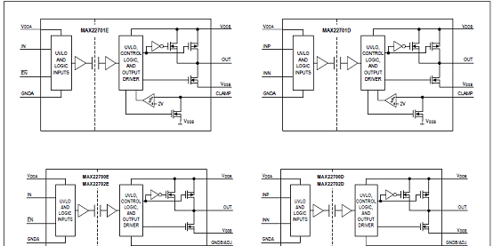
图1.MAX22700–MAX2270功能框图
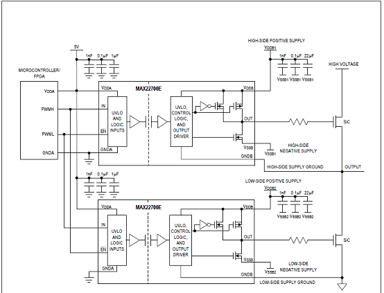
图2.MAX22700–MAX2270典型工作电路
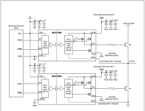
图3.MAX22700应用电路
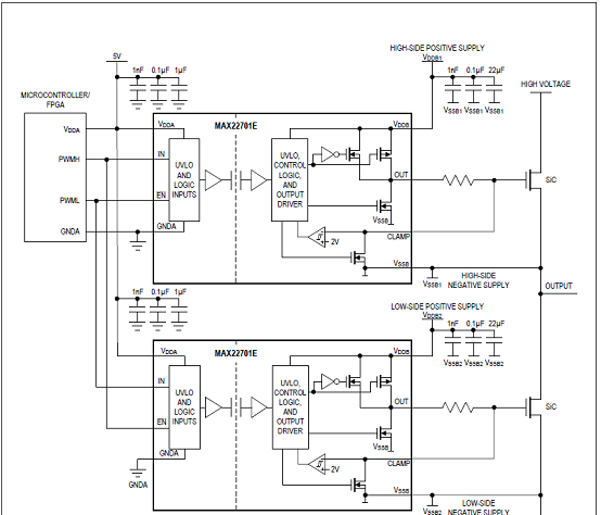
图4.MAX22701E应用电路
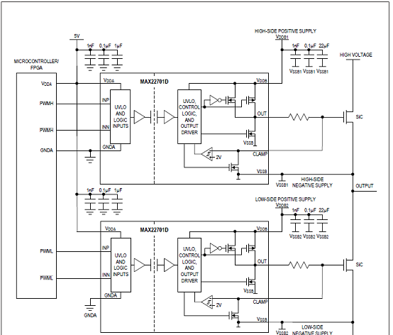
图5.MAX22701D应用电路

图6.MAX22702E应用电路
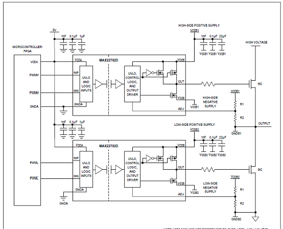
图7.MAX22702D应用电路
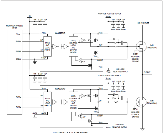
图8.MAX22701D应用电路
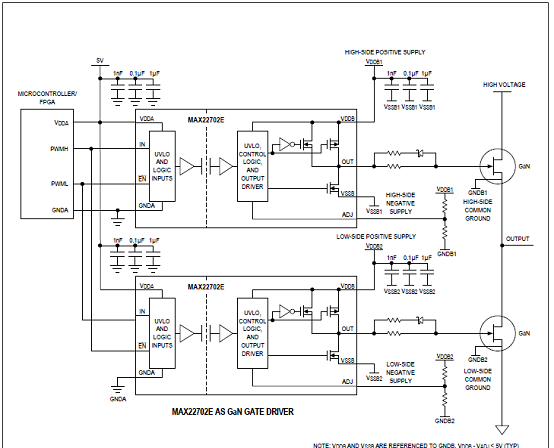
图9.MAX22702E应用电路
评估板MAX22700–MAX22702 EVK
The MAX22700–MAX22702 evaluation kits (EV kits) provide a proven design to evaluate the MAX22700– MAX22702 family of single-channel isolated gate drivers with ultra-high common-mode transient immunity (CMTI) of 300kV/μs (typ). Two identical channels (devices) are included on the EV kit in order to demonstrate the very tight part-to-part propagation delay matching of 2ns (max) over the -40℃ to +125℃ operating temperature range.
Two types of evaluation kits, MAX22701EVKIT# and MAX22702EVKIT#, are available to support variants with different B-side options, gate driver common pin GNDB (MAX22700), Miller Clamp pin (MAX22701), and adjustable undervoltage-lockout pin (MAX22702). In addition, both EV kits support variants with different A-side options, differential inputs (D versions), or a single-ended input with an enable pin (E versions). Both evaluation boards come with the narrow-body 8-pin SOIC package type. This board also supports the MAX22701DASA+, but requires the user to replace U1 and U2.
The MAX22702EVKIT# is fully assembled and tested, and comes populated with the MAX22702EASA+. This board also supports the MAX22700DASA+, MAX22700EASA+, and MAX22702DASA+ if the user replaces U1, U2, and necessary external components on the B side.
The EV kits should be powered from multiple independent isolated power supplies as required by the different power domains. The A side of the MAX22700–MAX22702 family has a nominal supply-voltage range from 3V to 5.5V. The B side has a nominal supply-voltage range of 13V to 36V or 6V to 36V depending upon the target device. For evaluating the electrical parameters of the devices without any isolation between the two sides and two devices, a common ground can be shared among different power domains.
评估板MAX22700–MAX22702 EVK主要特性:
2 EV Kits to Support 3 Output Options: GNDB, Miller Clamp, or Adjustable UVLO
2 Input Configurations: Single-Ended with Enable, or Differential
2 Identical Channels Allowing Propagation Delay Matching Measurements
2 Calibration Channels for Precision Propagation Delay Measurements
SMA Connectors and Terminal Blocks for Easy Connection to External Equipment
Wide Power Supply Voltage Range from 3V to 5.5V (A Side) and 13V to 36V (B Side)
Guaranteed Up to 3kVRMS Isolation for 60s
-40℃ to +125℃ Temperature Range
Proven PCB Layout

图10.评估板MAX22700–MAX22702 EVK外形图
左:评估板MAX22701E EVK外形图; 右:评估板MAX22702E EVK外形图
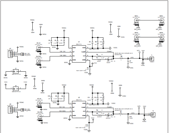
图11.评估板MAX22701 EVK电路图
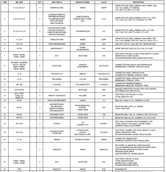
评估板MAX22701 EVK材料清单:

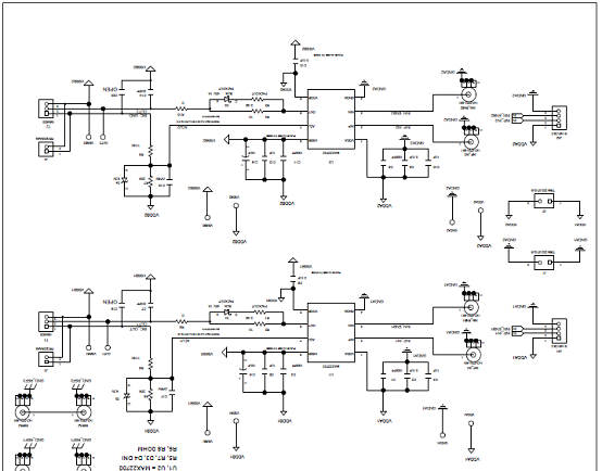
图15.评估板MAX22702 EVK电路图
评估板MAX22702 EVK材料清单:
责任编辑:David
【免责声明】
1、本文内容、数据、图表等来源于网络引用或其他公开资料,版权归属原作者、原发表出处。若版权所有方对本文的引用持有异议,请联系拍明芯城(marketing@iczoom.com),本方将及时处理。
2、本文的引用仅供读者交流学习使用,不涉及商业目的。
3、本文内容仅代表作者观点,拍明芯城不对内容的准确性、可靠性或完整性提供明示或暗示的保证。读者阅读本文后做出的决定或行为,是基于自主意愿和独立判断做出的,请读者明确相关结果。
4、如需转载本方拥有版权的文章,请联系拍明芯城(marketing@iczoom.com)注明“转载原因”。未经允许私自转载拍明芯城将保留追究其法律责任的权利。
拍明芯城拥有对此声明的最终解释权。
相关资讯
:
基于MC33771主控芯片的新能源锂电池管理系统解决方案

AMIC110 32位Sitara ARM MCU开发方案

基于AMIC110多协议可编程工业通信处理器的32位Sitara ARM MCU开发方案

基于展讯SC9820超低成本LTE芯片平台的儿童智能手表解决方案

基于TI公司的AM437x双照相机参考设计

基于MTK6580芯片的W2智能手表解决方案


 2012- 2022 拍明芯城ICZOOM.com 版权所有 客服热线:400-693-8369 (9:00-18:00)


