


 产品分类
产品分类
Cypress CY8C52 超低功耗PSoC系列开发方案
 216
216
 拍明
拍明
原标题:Cypress CY8C52 超低功耗PSoC系列开发方案
Cypress 公司的CY8C52 超低功耗PSoC系列采用32位PSoC 5平台,在CPU子系统周围提供了可编程的数字,模拟和互连区块.它的 32位 ARM Cortex-M3 CPU核工作在DC-40MHz,闪存程序存储器高达256KB,SRAM存储器高达64KB,2KB EEPROM,有多层AHB总线接入的24路DMA,工作电压0.5 V 到 5.5 V, 可以广泛应用在消费类电子,工业控制和医疗设备等各种领域..本文介绍了CY8C52系列主要特性, 简化方框图, ARM Cortex-M3 CPU框图, 时钟子系统框图,GPIO框图, 数字系统接口框图和模拟子系统框图,以及CY8CKIT-001 PSoC®开发套件主要特性, CY8CKIT-001 PSoC 开发板电路图, CY8C28, CY8C38和CY8C55系列处理器模块电路图与相应的材料清单.
With its unique array of configurable blocks, PSoC® 5 is a true system level solution providing MCU, memory, analog, and digital peripheral functions in a single chip. The CY8C52 family offers a modern method of signal acquisition, signal processing, and control with high accuracy, high bandwidth, and high flexibility. Analog capability spans the range from thermocouples (near DC voltages) to ultrasonic signals. The CY8C52 family can handle dozens of data acquisition channels and analog inputs on every GPIO pin. The CY8C52 family is also a high performance configurable digital system with some part numbers including interfaces such as USB, multi-master I2C, and CAN. In addition to communication interfaces, the CY8C52 family has an easy to configure logic array, lexible routing to all I/O pins, and a high performance 32-bit ARM® Cortex™-M3 microprocessor core. Designers can easily create system level designs using a rich library of prebuilt components and boolean primitives using PSoC® Creator™, a hierarchical schematic design entry tool. The CY8C52 family provides unparalleled opportunities for analog and digital bill of materials integration while easily accommodating last minute design changes through simple firmware updates.
CY8C52 主要特性:
• 32-bit ARM Cortex-M3 CPU core
DC to 40 MHz operation
Flash program memory, up to 256 KB, 100,000 write cycles, 20 year retention, multiple security features
Up to 64 KB SRAM memory
2 KB EEPROM memory, 1 million cycles, 20 years retention
24 channel DMA with multilayer AHB bus access
• Programmable chained descriptors and priorities
• High bandwidth 32-bit transfer support
Low voltage, ultra low power
Wide operating voltage range: 0.5 V to 5.5 V
High efficiency boost regulator from 0.5 V input to 1.8 V to 5.0 V output
2 mA at 6 MHz
Low power modes including:
• 2 μA sleep mode with real time clock and low voltage detect (LVD) interrupt
• 300 nA hibernate mode with RAM retention
Versatile I/O system
28 to 72 I/O (62 GPIO, 8 SIO, 2 USBIO[1])
Any GPIO to any digital or analog peripheral routability
LCD direct drive from any GPIO, up to 46x16 segments
CapSense® support from any GPIO[4]
1.2 V to 5.5 V I/O interface voltages, up to 4 domains
Maskable, independent IRQ on any pin or port
Schmitt trigger TTL inputs
All GPIO configurable as open drain high/low, pull up/down, High-Z, or strong output
Configurable GPIO pin state at power on reset (POR)
25 mA sink on SIO
Digital peripherals
20 to 24 programmable PLD based Universal Digital Blocks
Full CAN 2.0b 16 RX, 8 TX buffers[1]
Full-Speed (FS) USB 2.0 12 Mbps using internal oscillator[1]
Four 16-bit configurable timer, counter, and PWM blocks
Library of standard peripherals
• 8, 16, 24, and 32-bit timers, counters, and PWMs
• SPI, UART, I2C
• Many others available in catalog
Library of advanced peripherals
• Cyclic Redundancy Check (CRC)
• Pseudo Random Sequence (PRS) generator
• LIN Bus 2.0
• Quadrature decoder
Analog peripherals (1.71 V VDDA 5.5 V)
1.024 V±0.1% internal voltage reference across -40 C to +85 C (14 ppm/_ C)
SAR ADC, 12-bit at 1 Msps
One 8-bit, 8 Msps IDAC or 1 Msps VDAC
Two comparators with 75 ns response time
CapSense support
Programming, debug, and trace
JTAG (4 wire), Serial Wire Debug (SWD) (2 wire), Single Wire Viewer (SWV), and TRACEPORT interfaces
Cortex-M3 flash Patch and Breakpoint (FPB) block
Cortex-M3 Embedded Trace Macrocell™ (ETM™) generates an instruction trace stream.
Cortex-M3 Data Watchpoint and Trace (DWT) generates data trace information
Cortex-M3 Instrumentation Trace Macrocell (ITM) can be used for printf-style debugging
DWT, ETM, and ITM blocks communicate with off-chip debug and trace systems via the SWV or TRACEPORT
Bootloader programming supportable through I2C, SPI, UART, USB, and other interfaces
Precision, programmable clocking
3 to 24 MHz internal oscillator over full temperature and voltage range
4 to 33 MHz crystal oscillator for crystal PPM accuracy
Internal PLL clock generation up to 40 MHz
32.768 kHz watch crystal oscillator
Low power internal oscillator at 1, 33, and 100 kHz
Temperature and packaging
-40 C to +85 C degrees industrial temperature
68-pin QFN and 100-pin TQFP package options
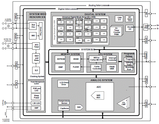
图.CY8C52简化方框图
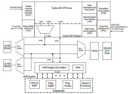
图.CY8C52 ARM Cortex-M3 框图
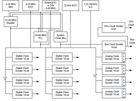
图.CY8C52 时钟子系统框图
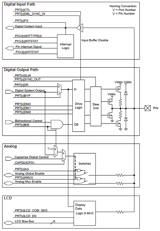
图.CY8C52 GPIO 框图
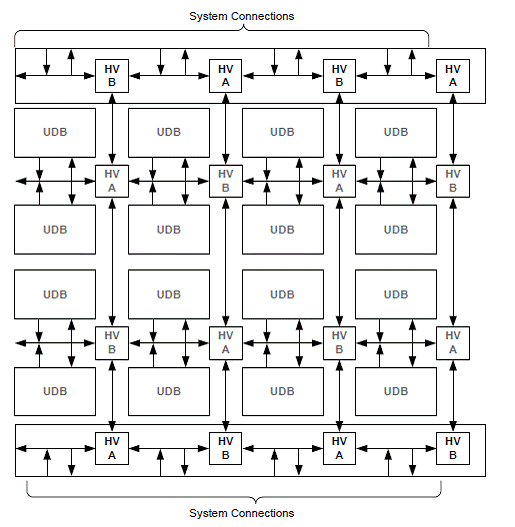
图.CY8C52 数字系统接口框图
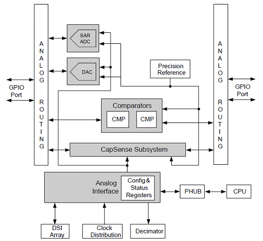
图.CY8C52 模拟子系统框图
CY8CKIT-001 PSoC®开发套件
The CY8CKIT-001 PSoC® Development Kit provides you a common development platform where you can prototype and evaluate different solutions using any one of the PSoC 1, PSoC 3, or PSoC 5 architectures. This guide and kit gives you a practical understanding of PSoC technology. In addition, the kit gives several example projects with step-by-step instructions to enable you to easily get started developing PSoC solutions. This kit includes PSoC CY8C28, CY8C38, and CY8C55 Family Processor Modules.
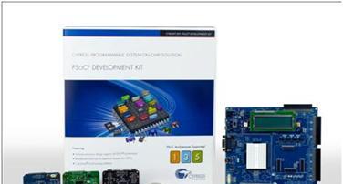
图.CY8CKIT-001 PSoC®开发套件外形图
The CY8CKIT-001 PSoC Development Kit includes:
■ PSoC Development Board
■ PSoC CY8C28 Family Processor Module
■ PSoC CY8C38 Family Processor Module
■ PSoC CY8C55 Family Processor Module
■ MiniProg3 Programmer and Debug tool
■ USB Cable
■ 12V Power Supply Adapter
■ Wire Pack
■ Printed Documentation
❐ Quick Start
❐ Schematic PSoC Development Board Design
■ Software CD for PSoC 1, which includes
❐ PSoC® Designer™ IDE
❐ PSoC® Programmer™ Software
❐ CY8C28 Data Sheets
❐ Kit Release Notes
❐ Software Release Notes
❐ Example Project Files, Firmware, And Documentation
■ Software CD for PSoC 3 / PSoC 5, which includes
❐ PSoC® Creator™ IDE
❐ PSoC Programmer Software
❐ CY8C38 Data Sheet
❐ CY8C55 Data Sheet
❐ Kit Release Notes
❐ Software Release Notes
❐ Example Project Files, Firmware, And Documentation
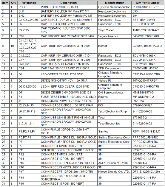
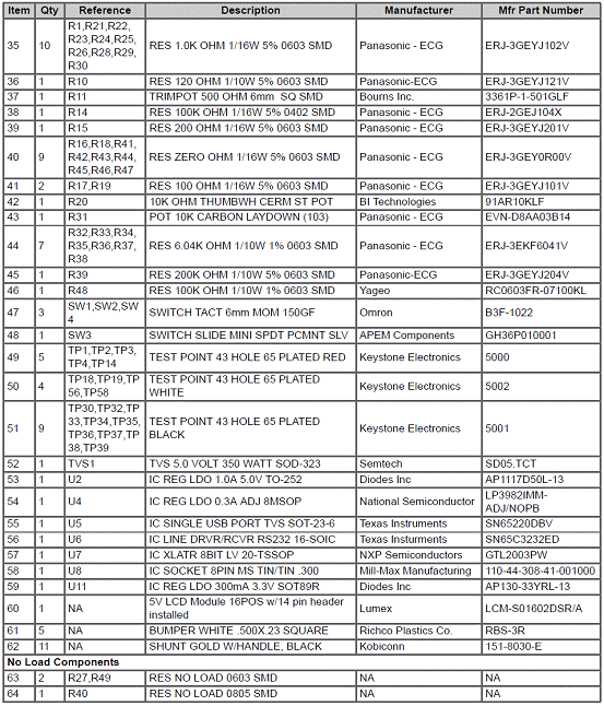
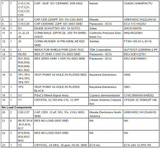
CY8CKIT-001 PSoC开发板材料清单(BOM):
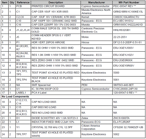
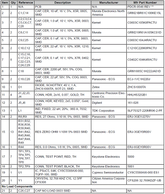
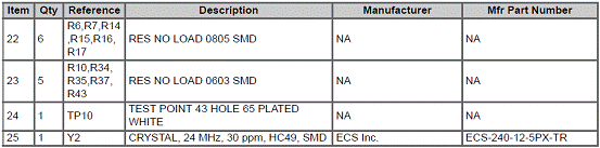
CY8C28 系列处理器模块材料清单(BOM):
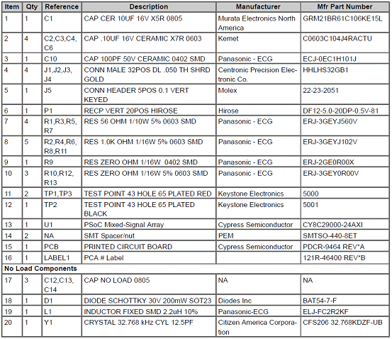
CY8C29 系列处理器模块材料清单(BOM):
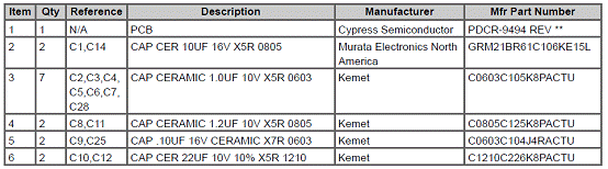
CY8C38 系列处理器模块材料清单(BOM):
CY8C55 系列处理器模块材料清单(BOM):
责任编辑:David
【免责声明】
1、本文内容、数据、图表等来源于网络引用或其他公开资料,版权归属原作者、原发表出处。若版权所有方对本文的引用持有异议,请联系拍明芯城(marketing@iczoom.com),本方将及时处理。
2、本文的引用仅供读者交流学习使用,不涉及商业目的。
3、本文内容仅代表作者观点,拍明芯城不对内容的准确性、可靠性或完整性提供明示或暗示的保证。读者阅读本文后做出的决定或行为,是基于自主意愿和独立判断做出的,请读者明确相关结果。
4、如需转载本方拥有版权的文章,请联系拍明芯城(marketing@iczoom.com)注明“转载原因”。未经允许私自转载拍明芯城将保留追究其法律责任的权利。
拍明芯城拥有对此声明的最终解释权。
相关资讯
:
基于MC33771主控芯片的新能源锂电池管理系统解决方案

AMIC110 32位Sitara ARM MCU开发方案

基于AMIC110多协议可编程工业通信处理器的32位Sitara ARM MCU开发方案

基于展讯SC9820超低成本LTE芯片平台的儿童智能手表解决方案

基于TI公司的AM437x双照相机参考设计

基于MTK6580芯片的W2智能手表解决方案


 2012- 2022 拍明芯城ICZOOM.com 版权所有 客服热线:400-693-8369 (9:00-18:00)


