


 产品分类
产品分类
基于Cypress CYW20819的超低功耗BLE蓝牙5.0 SoC开发方案
 322
322
 拍明
拍明
原标题:Cypress CYW20819超低功耗BLE蓝牙5.0 SoC开发方案
Cypress公司的CYW20819是超低功耗BLE/BR/EDR蓝牙5.0系统级芯片(SoC),采用最高集成度以消除外接元件,使设备制造商降低产品占位面积和成本. CYW20819集成了超低功耗(ULP)BLE和增加音频功能,以增加可穿载和跟踪者的用户体验.器件提供业界最好的BLE和EDR的接收灵敏度.采用先进的设计技术和工艺技术以降低工作和空闲功率.器件支持BR,EDR 2Mbps和3 Mbps,支持eSCO,BLE和LE 2Mbps,可编TX功率高达+44dBm,具有极好的接收器灵敏度,BLE 1Mbps时为-95.5dBm.器件的微处理器采用功能强大的Arm® Cortex®-M和,最大功率速率96MHz,ROM的蓝牙堆栈可在没有外接MCU时单独运行,集成了256KB闪存和176KB RAM,具有AES-128和真随机号码发生器(TRNG),ROM中的安全功能包括ECDSA签名验证.器件的外设包括多达40个GPIO,I2C, I2S, UART和 PCM接口,两个Quad-SPI接口,多达28个模拟通路的辅助ADC,三轴正交信号译码器,通用计时器和PWM以及其实时时钟(RTC)和看门狗计时器(WDT),主要用在蓝牙网络,音频,语音,可穿载,鼠标,键盘,游戏控制台,遥控,家庭自动化以及各种物联网(IoT)应用.本文介绍了CYW20819主要特性,功能框图,CYW20819支持的主要蓝牙特性以及评估板CYW920819EVB-02主要特性,框图和电源架构图,电路图,材料清单和PCB设计图.
The CYW20819 is a best-in-class Bluetooth 5 single-chip solution targeted at Bluetooth Mesh, audio, voice, wearables, mice,keyboards, gaming consoles, remote controls, home automation, and a wide range of other Internet of Things (IoT)applications. The CYW20819 fully implements the Bluetooth Mesh 1.0 specification, and employs the highest level of integration toeliminate external components, allowing device makers to reduce product footprints and slash costs.
The CYW20819 integrates Ultra-Low Power (ULP) BLE along with the capability to add audio functionality to enhance the userexperience for wearables and trackers. It also provides best-in-class receiver sensitivity for both BLE and EDR. Using advanceddesign techniques and process technology to reduce active and idle power, the CYW20819 also addresses the needs of a diverseclass of low power Bluetooth 5-enabled devices that require minimal power consumption and compact size The device is intendedfor use in audio (source only, other than SCO), IOT, sensors (medical, home, security and industrial), and HID markets. The datasheetprovides details of the functional, operational, and electrical characteristics of the CYW20819 device. It is intended for hardware,design, application, and OEM engineers.
CYW20819主要特性:
■ Bluetooth Sub-System
❐Complies with Bluetooth Core Specification version 5.0
❐Includes support for BR, EDR 2 Mbps and 3 Mbps, eSCO,BLE, and LE 2 Mbps.
❐Programmable TX Power up to +4 dBm
❐Excellent receiver sensitivity (-95.5 dBm for BLE 1 Mbps)
■ Microcontroller
❐Powerful Arm® Cortex®-M4 core with a maximum speed of96 MHz
❐Bluetooth stack in ROM allowing standalone operation withoutany external MCU
❐256-KB on-chip Flash
❐176-KB on-chip RAM
❐Bluetooth stack, Peripheral drivers, Security functions builtinto ROM (1 MB) allowing application to efficiently use onchipFlash
❐AES-128 and True Random Number Generator (TRNG)
❐Security functions in ROM including ECDSA signature verification
❐Over-the-air (OTA) firmware updates
■ Peripherals
❐Up to 40 GPIOs
❐I2C, I2S, UART, and PCM interfaces
❐Two Quad-SPI interfaces
❐Auxiliary ADC with up to 28 analog channels
❐Programmable key scan 20 8 matrix
❐Three-axis quadrature signal decoder
❐General-purpose timers and PWM
❐Real-time clock (RTC) and watchdog timers (WDT)
■ Power Management
❐On-chip power-on reset (POR)
❐Integrated buck (DC-DC) and LDO regulators
❐On-chip software controlled power management unit
❐On-chip 32 kHz LPO with optional external 32 kHz crystaloscillator support
■ Wi-Fi Coexistence
❐Global Coexistence Interface (GCI) for Cypress Wi-Fi parts
❐Serial Enhanced Coexistence Interface (SECI)
■ ModusToolBox 1.1 SDK
■ OTA Firmware Update Support
■ Package Types
❐112-ball FPBGA
❐62-pin FPBGA
❐RoHS compliant
CYW20819应用:
■ Wearables and fitness bands
■ Home automation
■ Blood pressure monitors and other medical applications
■ Proximity sensors
■ Key fobs
■ Thermostats and thermometers
■ Toys
■ Remotes

图1.CYW20819功能框图
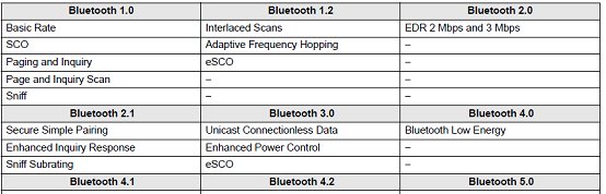
CYW20819支持的主要蓝牙特性:
评估板CYW920819EVB-02
Thank you for your interest in the CYW920819EVB-02 Evaluation Kit. CYW920819EVB-02 enables customers to evaluateand develop single-chip Bluetooth and Bluetooth Low Energy (BLE) applications using the CYW20819, dual-mode Bluetooth 5.0 (BLE and BR/EDR) wireless MCU.
CYW920819EVB-02 can be used with ModusToolbox™ software to develop and debug your CYW20819 project. The EVBoffers footprint-compatibility with Arduino™ shields. The development environment is compatible with Windows, macOSand Linux operating systems. In addition, the kit features an onboard programmer and USB-UART chip. The EVB supports1.8 V and 3.3 V operation.
评估板CYW920819EVB-02包括:
CYW920819EVB-02 evaluation board
USB 2.0 Type-A to micro-B cable
Quick Start Guide

图2.评估板CYW920819EVB-02套件图
评估板CYW920819EVB-02主要特性:
1. CYW20819 carrier module with on-board antenna*
2. Expansion headers compatible with Arduino shields
3. Support for 1.8 V, 3.3 V and coin cell operation of the CYW20819 device
4. Recovery button (Red), Reset button (Blue) and User button (Black)
5. On-board micro-USB connector (J6) for programming and debug purposes
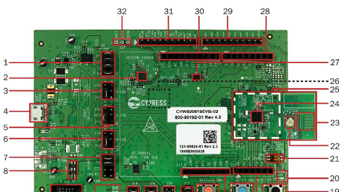
图3.评估板CYW920819EVB-02外形图(正面)
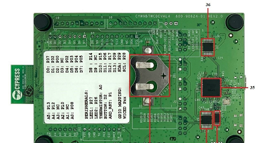
图4.评估板CYW920819EVB-02外形图(背面)
1. HCI UART Header (J5): This header can be used to connect or disconnect HCI UART from the USB-Serial device.
2. Motion Sensor (U2): This is an I2C-based 9-axis inertial motion sensor.
3. VDDIO Select Jumper (J7): This header is used to select the VDDIO power source. Possible selections are 3.3 V, 1.8
V, or VCOIN, which is the coin cell power supply on the bottom side of the board.
4. USB Connector (J6): J6 is a micro-B USB female connector for connecting the kit to PC using the provided USB cable.It is used for programming and USB-UART communication.
5. VBATT Select Header (J8): This header is used to select the VBATT (Core power supply) power source. The possibleselections are 3.3 V, 1.8 V, or VCOIN which is the coin cell power supply on the bottom side of the board.
6. VPA_BT Select Header (J16): This header is used to select the VPA_BT (Power Amplifier supply) power source. Thisselect header applies to evaluation boards that has an external power amplifier and it is not connected to CYW20819in CYW920819EVB-02 evaluation board.
7. PUART Header (J10): This header can be used to connect or disconnect the PUART pins from the USB-Serial device.
8. SWD/GPIO Switch (SW9): This DIP switch allows you to route the functionality of GPIO/SWD lines to either J4 Arduinocompatibleheader or the J13 debug header.
9. Debug Header (J13): J13 is a 10-pin interface header that can be used to connect an external debugger via SWD.
10. Thermistor (R30): The onboard thermistor is an NTC analog thermistor that can be used to measure temperature.
11. Thermistor Enable Header (J14): This jumper can be used to connect or disconnect the on-board thermistor from theCYW20819 device.
12. Peripheral Enable (J18): The jumper allows the user to disconnect the VDDIO supply to onboard peripheral deviceslike motion sensor, thermistor, analog mic and real-time clock by disabling VDDP.
13. EXT_LPO Enable Jumper (J19): This jumper is open by default. When the jumper is closed, the RTC (G1 in schematics) provides a 32.768-kHz clock source to the CYW20819’s EXT_LPO pin. When the jumper is open, the Y2 crystal provides 32.768-kHz to XTAL_32K(I/O) pins of CYW20819. To use the EXT_LPO instead of Y2 crystal, the user needs to remove the entire Y2 circuit which includes R6, Y2, C19 and C20 and populate R7 with zero-ohm resistor.
14. VDDIO Current Measurement Header (J15): This jumper is used to power the carrier module. To measure the currentconsumed by the carrier module, remove this jumper and connect an ammeter to the two pins.
15. Recovery Button (SW1): This button is used to put the device in recovery mode. To put the device in recovery mode,press and hold the recovery button, press and release the reset button, and then release the recovery button. The usermay need to put the device in recovery mode when the application download fails.
16. Arduino Compatible Header (J11): The Arduino-compatible I/O header brings out pins from CYW20819 to interfacewith Arduino shields.
17. Reset Button (SW2): This button can be used to reset the device.
18. Arduino Compatible Header (J12): The Arduino-compatible I/O header brings out pins from CYW20819 to interfacewith Arduino shields.
19. User Button (SW3): This button can be used to provide an input to the CYW20819 device. Note that the buttonconnects the CYW20819 pin to ground when pressed; therefore, the CYW20819 pin must be configured as a digitalinput with resistive pull-up for detecting the button press.
20. User LEDs (D1 and D2): These on-board LEDs can be controlled by the CYW20819 device. The LEDs are activeLOW; therefore, these pins must be driven to ground to turn ON the LEDs.
21. LED Enable Switch (SW4): These DIP switches are used to connect/disconnect the user-controlled LEDs from theCYW20819 device.
22. External Antenna Connector (U1.J3): The external antenna connector is an RF connector fed from the BT_RFIOpad of the CYW20819 followed by a band pass filter. See Hardware Design Guidelines for more details.
23. PCB Antenna (A1): The PCB antenna is the EM wave radiating part of the evaluation board which is fed from theBT_RF pad of CYW20819 followed by a band pass filter and an antenna matching circuit.
24. CYW20819(U1. U1): The Bluetooth (BR/EDR- Basic Rate and Enhanced Data Rate) and Bluetooth Low Energy 5qualified system-on-chip from Cypress is the heart of this evaluation kit.
25. Carrier Module (U1): The carrier module has the CYW20819 SoC on it. A Bluetooth antenna is etched on the carriermodule PCB. The UART and GPIOs are brought out from the SoC pads to interface with the baseboard.
26. Coin Cell Holder (ZB1): This is a coin cell battery holder located on the bottom side of the development kit. If theevaluation board needs to use the power supplied from the coin cell, then the VDDIO and VBAT select headers mustbe set to VCOIN.
27. 8-Mb Serial Flash (U6): This is the 8-Mbit SPI flash used for application purpose.
28. Arduino Compatible Header (J4): The Arduino-compatible I/O header brings out pins from CYW20819 to interfacewith Arduino shields.
29. WICED Header (J2): This header brings out some pins of the CYW20819 device that are not connected to the Arduinocompatible headers. These pins can be used for testing or for custom applications.
30. Arduino Compatible Header (J3): The Arduino-compatible I/O header brings out pins from CYW20819 to interfacewith Arduino shields.
31. WICED Header (J1): This header brings out some pins of the CYW20819 device that are not connected to the Arduinocompatible headers. These pins can be used for testing or for custom applications.
32. Motion Sensor Interrupt Test points (J17): This header has three test points for probing the interrupts from the motionsensor (U2).
33. PUART Voltage Level Translator (U9): This voltage level translator IC allows the interoperability of devices(CYW20819 device and USB/Serial IC) with different high-level and low-level voltages for input and output operations.
34. EEPROM (U10): This EEPROM contains the configuration information for the USB to UART Converter for acting as a USB Slave device.
35. USB to UART converter (U8): This is a 2-channel USB to UART IC for communicating between CYW20819 and a PC
BT UART (HCIUART) Voltage Level Translator (U7): This voltage level translator IC allows interoperability of devices (CYW20819 device and USB/Serial IC) with different high-level and low-level voltages for input and output operations.
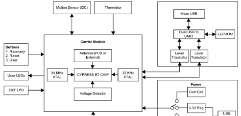
图5.评估板CYW920819EVB-02框图
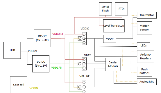
图6.评估板CYW920819EVB-02电源架构图
责任编辑:David
【免责声明】
1、本文内容、数据、图表等来源于网络引用或其他公开资料,版权归属原作者、原发表出处。若版权所有方对本文的引用持有异议,请联系拍明芯城(marketing@iczoom.com),本方将及时处理。
2、本文的引用仅供读者交流学习使用,不涉及商业目的。
3、本文内容仅代表作者观点,拍明芯城不对内容的准确性、可靠性或完整性提供明示或暗示的保证。读者阅读本文后做出的决定或行为,是基于自主意愿和独立判断做出的,请读者明确相关结果。
4、如需转载本方拥有版权的文章,请联系拍明芯城(marketing@iczoom.com)注明“转载原因”。未经允许私自转载拍明芯城将保留追究其法律责任的权利。
拍明芯城拥有对此声明的最终解释权。
相关资讯
:
基于MC33771主控芯片的新能源锂电池管理系统解决方案

AMIC110 32位Sitara ARM MCU开发方案

基于AMIC110多协议可编程工业通信处理器的32位Sitara ARM MCU开发方案

基于展讯SC9820超低成本LTE芯片平台的儿童智能手表解决方案

基于TI公司的AM437x双照相机参考设计

基于MTK6580芯片的W2智能手表解决方案


 2012- 2022 拍明芯城ICZOOM.com 版权所有 客服热线:400-693-8369 (9:00-18:00)


