


 产品分类
产品分类
TI AM6548 Sitara MCU多协议吉比特工业4.0解决方案
 122
122
 拍明
拍明
原标题:TI AM6548 Sitara MCU多协议吉比特工业4.0解决方案
TI公司的AM6548是具有TSN使能的用于工业4.0 工业级Sitara处理器, 提供先进工业通信,增强安全性,高度可靠性和安全特性.处理器组合两个四个或两个ARM Cortex-A53和和两个Cortex-R5F MCU子系统, 四核Arm® Cortex®-A53 MCU工作频率高达1.1GHz,双核Arm Cortex-R5F MCU工作频率高达400MHz,具有三个吉比特工业通信子系统(PRU_ICSSG),两个10/100/1000以太网端口 per PRU_ICSSG,支持两个SGMII端口,和10/100Mb PRU-ICSS兼容,有24x PWM per PRU_ICSSG,可以逐个周期控制,主要用在工业可编控制器(PLC),带安全功能的工厂自动化,多协议现场总线通信,工业PC,工业机器人,人机接口,电网基础设备保护继电器和机器人马达驱动器.本文介绍了AM654x和AM652x主要特性,功能框图,以及TMDX654GPEVM AM65x 评估模块(EVM)系统外形图和处理器板电路图,材料清单和PCB设计图.
AM654x and AM652x Sitara Arm applications processors are built to meet the complex processing needs of modern industrial embedded products.
The AM654x and AM652x devices combine four or two Arm Cortex-A53 cores with a dual Cortex-R5F MCU subsystem which includes features intended to help customers achieve their functional safety goals for their end products and three Gigabit industrial communications subsystems (PRU_ICSSG) to create a SoC capable of high-performance industrial controls with industrial connectivity and processing for functional safety applications. AM65xx is currently undergoing assessment to be certified by TÜV SÜD
according to IEC 61508.
The four A53 cores are arranged in two dual-core clusters with shared L2 memory to create two processing channels. Extensive ECC is included on on-chip memory, peripherals, and interconnect for reliability. The SoC as a whole includes features intended to help customers design systems that can achieve their functional safety goals (assessment pending with TÜV SÜD). Cryptographic acceleration and secure boot are available on AM654x and AM652x devices in addition to granular firewalls managed by the DMSC.
Programmability is provided by the quad-core Arm Cortex-A53 RISC CPUs with Neon extension, and the dual Cortex-R5F MCU subsystem is available for general purpose use as two cores or it can be used in lockstep to help meet the needs of functional safety applications. The PRU_ICSSG subsystems can be used to provide up to six ports of industrial Ethernet such as Profinet IRT, TSN, or EtherCAT™ (among many others), or they can be used for standard Gigabit Ethernet connectivity.
TI provides a complete set of software and development tools for the Arm cores including Processor SDK Linux-RT, RTOS, and Android as well as C compilers and a debugging interface for visibility into source code execution. Applicable safety documentation will be made available to assist customers in developing their functional safety related systems.
AM654x和AM652x主要特性:
1Processor Cores:
• Quad-Core Arm® Cortex®-A53 Microprocessor Subsystem at up to 1.1 GHz
– Two Dual-Core Cortex-A53 Clusters with 512KB L2 Cache Including SECDED
– Each A53 Core has 32KB L1 ICache and 32K L1 DCache
• Dual-Core Arm Cortex-R5F at up to 400 MHz
– Supports Lockstep Mode
– 16KB ICache, 16KB DCache, and 64KB RAM per R5F Core
Industrial Subsystem:
• Three Gigabit Industrial Communication Subsystems (PRU_ICSSG)
– Two 10/100/1000 Ethernet Ports per PRU_ICSSG
– Supports Two SGMII Ports (2)
– Compatibility with 10/100Mb PRU-ICSS
– 24× PWMs per PRU_ICSSG
– Cycle-by-Cycle Control
– Enhanced Trip Control
– 18× Sigma-Delta Filters per PRU_ICSSG
– Short Circuit Logic
– Over-Current Logic
– 6× Multi-protocol Position Encoder Interfaces per PRU_ICSSG
Memory Subsystem:
• Up to 2MB of On-Chip L3 RAM with SECDED
• Multi-Core Shared Memory Controller (MSMC)
– Up to 2MB (2 banks × 1MB) SRAM with SECDED
– Shared Coherent Level 2 or Level 3 Memory-Mapped SRAM
– Shared Coherent Level 3 Cache
– 256-Bit Processor Port Bus and 40-Bit Physical Address Bus
– Coherent Unified Bi-Directional Interfaces to Connect to Processors or Device Masters
– L2, L3 Cache Pre-Warming and Post Flushing
– Bandwidth Management with Starvation Bound
– One Infrastructure Master Interface
– Single External Memory Master Interface
– Supports Distributed Virtual System
– Supports Internal DMA Engine – DRU (Data Routing Unit)
– ECC Error Protection
• DDR Subsystem (DDRSS)
– Supports DDR3L/DDR4 Memory Types up to DDR-1600
– Supports LPDDR4 Memory Type up to DDR-1333
– 32-Bit Data Bus and 7-Bit SECDED Bus
– 32GB of Total Addressable Space
• General-Purpose Memory Controller (GPMC)
Safety:
• AM65xx Helps System Designers Address Safety Requirements
– The Dual Cortex-R5F System is Undergoing Assessment to be Certified at TÜV SÜD
According to IEC 61508, Targeting SIL-3
– The A53 Cores and Entire System on Chip (SoC) is Undergoing Assessment to be Certified at TÜV SÜD According to IEC 61508, Targeting SIL-2
– ECC or Parity on Calculation-Critical Memories
– ECC and Parity on Internal Bus Interconnect
– Firewalls to Help Provide Freedom From Interference (FFI)
– Built-In Self-Test (BIST) for CPU, High-End Timers, and On-Chip RAM
– Hardware Error Injection Support for Test-for- Diagnostics
– Error Signaling Modules (ESM) for Capture of Safety Related Errors
– Voltage, Temperature, and Clock Monitoring
– Windowed and Non-Windowed Watchdog Timers in Multiple Clock Domains
• MCU Island
– Isolation of the Dual-Core Arm Cortex-R5F Microprocessor Subsystem to Help Provide
Freedom From Interference (FFI)
– Separate Voltage, Clocks, Resets, and Dedicated Peripherals
– Internal MCSPI Connection to the Rest of SoC
Security:
• Secure Boot Supported
– Hardware-Enforced Root-of-Trust
– Support to Switch Root-of-Trust via Backup Key
– Support for Takeover Protection, IP Protection, and Anti-Roll Back Protection
• Cryptographic Acceleration Supported
– Session-Aware Cryptographic Engine with Ability to Auto-Switch Key-Material Based on
Incoming Data Stream
– Supports Cryptographic Cores
– AES – 128/192/256 Bits Key Sizes
– 3DES – 56/112/168 Bits Key Sizes
– MD5, SHA1
– SHA2 – 224/256/384/512
– DRBG with True Random Number Generator
– PKA (Public Key Accelerator) to Assist in RSA/ECC Processing
– DMA Support
• Debugging Security
– Secure Software Controlled Debug Access
– Security Aware Debugging
• Trusted Execution Environment (TEE) Supported
– Arm TrustZone® Based TEE
– Extensive Firewall Support for Isolation
– Secure DMA Path and Interconnect
– Secure Watchdog/Timer/IPC
• Secure Storage Support
• On-the-Fly Encryption and Authentication Support for OSPI Interface
• Networking Security Support for Data (Payload) Encryption/Authentication via Packet Based Hardware Cryptographic Engine
• Security Co-Processor (DMSC) for Key and Security Management, with Dedicated Device Level Interconnect for Security
SoC Services:
• Device Management Security Controller (DMSC)
– Centralized SoC System Controller
– Manages System Services Including Initial Boot, Security, Safety and Clock/Reset/Power Management
– Power Management Controller for Active and Low Power Modes
– Communication with Various Processing Units over Message Manager
– Simplified Interface for Optimizing Unused Peripherals
– Tracing and Debugging Capability
• Sixteen 32-Bit General-Purpose Timers
• Two Data Movement and Control Navigator Subsystems (NAVSS)
– Ring Accelerator (RA)
– Unified DMA (UDMA)
– Up to 2 Timer Managers (TM) (1024 Timers Each)
Multimedia:
• Display Subsystem
– Two Fully Input-Mapped Overlay Managers Associated with Two Display Outputs
– One Port MIPI® DPI Parallel Interface
– One Port OLDI
• Graphics Processing Unit (GPU)
• One Camera Serial Interface-2 (MIPI CSI-2)
• One Port Video Capture: BT.656/1120 (No Embedded Sync)
High-Speed Interfaces:
• One Gigabit Ethernet (CPSW) Interface Supporting
– RMII (10/100) or RGMII (10/100/1000)
– IEEE1588 (2008 Annex D, Annex E, Annex F) with 802.1AS PTP
– Audio/Video Bridging (P802.1Qav/D6.0)
– Energy-Efficient Ethernet (802.3az)
– Jumbo Frames (2024 bytes)
– Clause 45 MDIO PHY Management
• Two PCI-Express® Revision 3.1 Subsystems (2)
– Supports Gen3 (8.0GT/s) Operation
– Two Independent 1-lane, or a Single 2-lane Port
– Support for Concurrent Root-Complex and/or End-Point Operation
• USB 3.1 Dual-Role Device Subsystem (2)
– One Enhanced SuperSpeed Gen1 Port
– One USB 2.0 Port
– Each Port Independently Configurable as USB Host, USB Peripheral, or USB Dual-Role Device
General Connectivity:
• 6× Inter-Integrated Circuit (I2C) Ports
• 5× Configurable UART/IrDA/CIR Modules
• Two Simultaneous Flash Interfaces Configured
– Two OSPI™ Flash Interfaces
– or Hyperbus™ and OSPI1 Flash Interface
• 2× 12-Bit Analog-to-Digital Converters (ADC)
– Up to 4 Msamples/s
– Eight Multiplexed Analog Inputs
• 8× Multichannel Serial Peripheral Interfaces (MCSPI) Controllers
– Two with Internal Connections
– Six with External Interfaces
• General-Purpose I/O (GPIO) Pins
Control Interfaces:
• 6× Enhanced High Resolution Pulse-Width Modulator (EHRPWM) Modules
• One Enhanced Capture (eCAP) Module
• 3× Enhanced Quadrature Encoder Pulse (eQEP) Modules
Automotive Interfaces:
• 2× Modular Controller Area Network (MCAN) Modules with Full CAN-FD Support
Audio Interfaces:
• 3× Multichannel Audio Serial Port (MCASP) Modules
Media and Data Storage:
• 2× MultiMedia Card/Secure Digital (MMC/SD) Interfaces
Simplified Power Management:
• Simplified Power Sequence with Full Support for Dual Voltage I/O
• Integrated LDOs Reduces Power Solution Complexity
• Integrated SDIO LDO for Handling Automatic Voltage Transition for SD Interface
• Integrated POR (Power on Reset) Generation Reducing Power Solution Complexity
• Integrated Voltage Supervisor for Safety Monitoring
• Integrated Power Supply Glitch Detector for Detecting Fast Power Supply Transients
Analog/System Integration:
• Integrated USB VBUS Detection
• Fail Safe I/O for DDR RESET
• All I/O Pins Drivers Disabled During Reset to Avoid Bus Conflicts
• Default I/O Pulls Disabled During Reset to Avoid System Conflicts
• Support Dynamic I/O Pinmux Configuration Change
System on Chip (SoC) Architecture:
• Supports Primary Boot from UART, I2C, MCSPI, HyperBus, Parallel NOR Flash, SD or eMMC, USB, PCIe, and Ethernet Interfaces
• 28-nm CMOS Technology
• 23 mm × 23 mm, 0.8-mm Pitch, 784-Pin S-PBGA (ACD)
AM654x和AM652x应用:
• Industrial Programmable Controllers (PLC)
• Factory Automation with Safety Functions
• Multi-Protocol Fieldbus Communications
• Industrial PC
• Industrial Robots
• Human Machine Interface (HMI)
• Grid Infrastructure Protection Relays
• Robotic Motor Drives
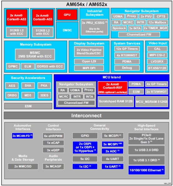
图1. AM654x和AM652x功能框图
The AM65x GP EVM is a standalone test, development, and evaluation module (EVM) system that lets developers write software and develop hardware for industrial communication-type applications. The GP EVM is equipped with AM6548 processor from TI and a defined set of features to let the user experience industrial communication solutions using serial, Ethernet-based, PCIe, and many other interfaces. Using standard interfaces, the GP EVM can communicate with other processors or systems, and act as a
communication gateway. In addition, the GP EVM can directly operate as a standard remote I/O system or simple sensor connected to an industrial communication network. The embedded emulation logic allows for emulation and debugging using standard development tools such as Code Composer Studio™, from TI, by using the supplied USB cable.
The AM65x GP EVM is a high performance, standalone development platform that enables users to evaluate and develop industrial applications for the Texas Instrument’s K3 System-on-Chip (SoC). The AM65x GP EVM supports the following key features:
• Based on the K3 architecture with Arm
• 4-GB DDR4 supporting data rate up to 1600 MT/s
• 16-GB eMMC Flash
• Full size SD card, up to 64-GB density with UHS-1 support (8-GB UHS-1 card supplied with the kit)
• 128-Mbit SPI EEPROM
• 512-Mbit OSPI EEPROM
• 256-Kbit I2C Boot EEPROM
• 3× PRU-ICSSG, supporting multi-protocol industrial Gigabit Ethernet on 2 ports
• Expansion Connectors with two full PRU-ICSSG ports
• 1x MCU Gigabit Ethernet port
• One USB2.0 interface port with Micro AB connector
• CSI-2 connector to interface camera card
• I-PEX EVAFLEX5-VS connector to interface with the LCD adapter card
• GPMC/DSS interface expansion connector
• Application board expansion connector
• SERDES expansion connector to interface two lane PCIe Personality card
• XDS110 on-board emulator
• Quad port UART to USB circuit over microB USB connector
• Expansion headers:
– Two UART
– One SPI
– One I2C
– Four timer signals
• Boot mode selection using DIP switches
• Two push buttons to generate interrupts
• Industrial Ethernet LEDs
• DC Input: 11 V to 28 V
• Status output: LEDs to indicate power status
• INA devices for current monitoring
• Over- and under-voltage protection circuit
• RoHS-compliant design
AM654x系列评估模块
The AM65x Evaluation Module provides a platform to quickly start evaluation of Sitara™ Arm® Cortex®-A53 AM65x Processors (AM6548, AM6546, AM6528, AM6527, AM6526) and accelerate development for HMI, networking, patient monitoring, and other industrial applications. It is a development platform based on the quad core Cortex-A53, dual Cortex-R5F processor that is integrated with ample connectivity such as PCIe, USB 3.0/2.0, Gigabit Ethernet, and more.
AM654x系列评估模块主要特性:
3 gigabit Ethernet ports
4GB DDR4 with ECC
On-board 16GB eMMC
On-board 512Mb OSPI Flash
1-lane PCIe Gen3.1, USB 3.1, USB 2.0 and CSI-2 interfaces
AM654x系列评估模块包括:
Assembled EVM
SD card
USB cable
Ethernet cable
Documentation
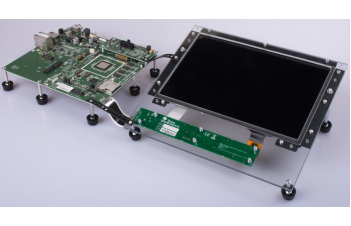
图2. TMDX654GPEVM AM65x 评估模块(EVM)系统外形图
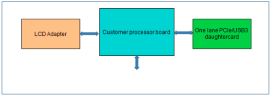
图3. TMDX654GPEVM AM65x 评估模块(EVM)系统架构接口图
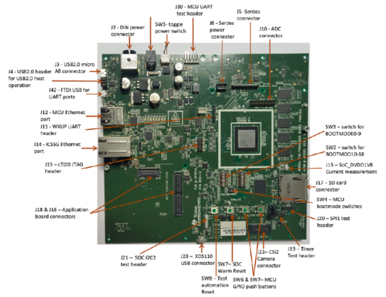
图4.处理器板外形图(顶视图)
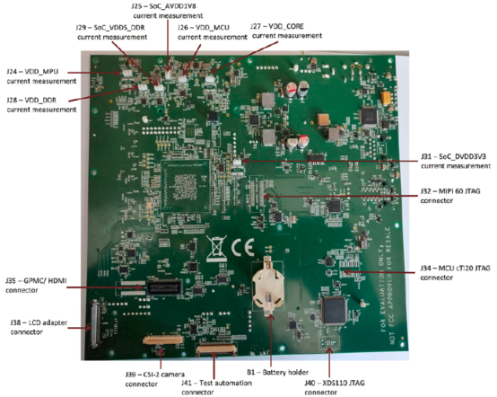
图5.处理器板外形图(底视图)
处理器板主要特性:
SoC:
• Based on the K3 architecture with Quad-Core Arm® Cortex®-A53 Microprocessor and Dual-Core Arm
Cortex-R5F Arm
• Heatsink and support for 12-V fan
Memory:
• 4-GB DDR4 supporting data rate up to 1600 MT/s
• 16-GB eMMC Flash which can support HS400 speed of operation
• Full size SD card, up to 64-GB density with UHS-1 support
• 128-Mbit SPI EEPROM
• 512-Mbit OSPI EEPROM
• 256-Kbit I2C EEPROM for Boot
I/O Interface:
• One MCU Gigabit Ethernet port and two Industrial Ethernet ports based on the Gigabit Industrial Communication Subsystem (PRU-ICSS-Gb) paired with Texas Instruments Gigabit Ethernet PHYs
• One USB2.0 interface with Micro AB connector
• CSI-2 connector to interface camera card
Expansion Bus:
• I-PEX EVAFLEX5-VS connector to interface with the LCD adapter card
• GPMC/DSS interface expansion connector for secondary display
• Application connector to expansion application cards
• SERDES expansion connector to support various SERDES modules
Debug:
• XDS110 on-board emulator
• Supports 20-pin JTAG connection from external emulator
• Automatic selection between on-board and external emulator (higher priority)
• Quad port UART to USB circuit over microB USB connector
• Two UART, one SPI, and I2C ports connected to test header for slave testing of the AM65x device
• Four timer signals from Maxwell connected to test header
• Two push buttons to generate Interrupts
Power Supply:
• Wide range DC input: 11 V to 28 V
• Status output: LEDs to indicate power status
• INA devices for current monitoring
• Over- and under-voltage protection circuit
Compliance:
• RoHS-compliant
• REACH-compliant
责任编辑:HanFeng
【免责声明】
1、本文内容、数据、图表等来源于网络引用或其他公开资料,版权归属原作者、原发表出处。若版权所有方对本文的引用持有异议,请联系拍明芯城(marketing@iczoom.com),本方将及时处理。
2、本文的引用仅供读者交流学习使用,不涉及商业目的。
3、本文内容仅代表作者观点,拍明芯城不对内容的准确性、可靠性或完整性提供明示或暗示的保证。读者阅读本文后做出的决定或行为,是基于自主意愿和独立判断做出的,请读者明确相关结果。
4、如需转载本方拥有版权的文章,请联系拍明芯城(marketing@iczoom.com)注明“转载原因”。未经允许私自转载拍明芯城将保留追究其法律责任的权利。
拍明芯城拥有对此声明的最终解释权。
相关资讯
:
基于MC33771主控芯片的新能源锂电池管理系统解决方案

AMIC110 32位Sitara ARM MCU开发方案

基于AMIC110多协议可编程工业通信处理器的32位Sitara ARM MCU开发方案

基于展讯SC9820超低成本LTE芯片平台的儿童智能手表解决方案

基于TI公司的AM437x双照相机参考设计

基于MTK6580芯片的W2智能手表解决方案


 2012- 2022 拍明芯城ICZOOM.com 版权所有 客服热线:400-693-8369 (9:00-18:00)


