


 产品分类
产品分类
Maxim MAX8655 25A同步PWM降压电源解决方案
 73
73
 拍明
拍明
原标题:Maxim MAX8655 25A同步PWM降压电源解决方案
Maxim公司的MAX8655是25A输出电流同步PWM降压电源稳压器,输入电压4.5V-25V,输出电压从0.7V到5.5V可调.集成的功率MOSFET提供小占位面积,容易布局和降低EMI等优点,主要用在POL电源,通信电源,网络设备,非隔离的DC/DC转换器,服务器和工作站,笔记本电脑,IBA电源等.本文介绍了MAX8655主要特性,方框图,多种典型应用电路以及MAX8655评估板电路图和材料清单(BOM).
The MAX8655 synchronous-PWM buck regulator operates from a 4.5V to 25V input and generates an output voltage adjustable from 0.7V to 5.5V at loads up to 25A.
Integrated power MOSFETs provide a small footprint, ease of layout, and reduced EMI. Removing the board trace inductances ensures the highest efficiency at high frequency.
The MAX8655 uses peak current-mode control architecture with an adjustable (200kHz to 1MHz), constantswitching frequency, which is externally synchronizable. The MAX8655’s adjustable current limit uses the inductor’s DC resistance to improve efficiency or an external sense resistor for higher accuracy. Foldback type current limit is available to reduce the power dissipation under severe-overload or short-circuit conditions. A reference input is provided for use with a high-accuracy external reference or for DDR and tracking applications.
Monotonic startup provides safe starting into a prebiased output, where traditional step-down regulators discharge the output capacitor during soft-start, creating a negative voltage at the output and possibly damaging the load.
A 180° out-of-phase synchronization output is available for synchronizing with another MAX8655. An enable input is provided for on/off control and to facilitate output sequencing. Output-voltage sensing for programmable overvoltage protection is provided and is independent of the feedback network to further enhance the output overvoltage protection.
Overall, the MAX8655 provides enough flexibility for the experienced user, as well as simplicity and ease of use for non-power-supply engineers.
MAX8655主要特性:
_ 25A Output Current
_ Integrated Power MOSFETs
_ Operates from 4.5V to 25V Supply
_ 1% FB Voltage Accuracy Over Temperature
_ Adjustable Output Voltage Down to 0.7V
_ Adjustable Switching Frequency and External Synchronization from 200kHz to 1MHz
_ 180° Phase-Shifted Synchronization
_ Adjustable Overcurrent Limit
_ Adjustable Slope Compensation
_ Selectable Current-Limit Mode: Latch-Off or Automatic Recovery
_ Monotonic Output Voltage Rise at Startup into Prebias Output
_ Output Sources and Sinks Current for DDR Applications
_ Enable Input
_ Power-OK (POK) Output
_ Adjustable Soft-Start
_ Independently Adjustable Overvoltage Protection
MAX8655应用:
Point-of-Load Power Supplies
Telecom Power
Networking
Nonisolated DC-DC Power Modules
Servers and Workstations
Notebook Computers
IBA Power Supplies

图1.MAX8655功能方框图

图2.MAX8655典型工作电路图

图3.MAX8655单相600kHz开关频率应用电路图:10.8V-13.2V输入,1.2V/20A输出

图4.MAX8655单相350kHz开关频率应用电路图:16V-20V输入,3.3V/20A输出
MAX8655评估板
The MAX8655 evaluation kit (EV kit) is a fully assembled and tested surface-mount PCB that contains a fixed-frequency, pulse-width modulated (PWM) stepdown switching regulator. The MAX8655 EV kit provides a 1.2V output voltage from a 10.8V to 13.2V input source and delivers up to 20A output current. The MAX8655 IC features internal high-side and lowside power MOSFETs.
A reference input is provided for use with a highaccuracy external reference (REFIN) or for DDR and tracking applications. The MAX8655 EV kit operates at 600kHz. The MAX8655 IC has a programmable internal oscillator with frequency range from 200kHz to 1MHz.
The MAX8655 can also be synchronized to an external clock by connecting the clock signal to FSYNC. A synchronization output (SYNCO) is provided to synchronize a second MAX8655 180° out-of-phase with the first by connecting SYNCO of the first MAX8655 to FSYNC of the second.
MAX8655评估板主要特性:
♦ 10.8V to 13.2V Input-Voltage Range
♦ 20A Maximum Output Current (Additional Airflow or Heat Sink May be Required Above 13A of Output Current)
♦ Adjustable Output from 0.7V to 5.5V
♦ Internal High-Side and Low-Side Power MOSFETs
♦ 200kHz to 1MHz Adjustable Switching Frequency and SYNC Input
♦ SYNCO Synchronizes 2nd Regulator 180° Out-of- Phase
♦ Monotonic Startup Provides Safe Starting Into a Pre-Biased Output
♦ Enable Input and Power-OK Signals
♦ Low-Profile Components
♦ Lead-Free and RoHS Compliant
♦ Fully Assembled and Tested

图5.MAX8655 EVK评估板电路图(1)

图6.MAX8655 EVK评估板电路图(2)
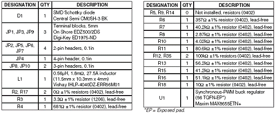
所用元件列表:

责任编辑:HanFeng
【免责声明】
1、本文内容、数据、图表等来源于网络引用或其他公开资料,版权归属原作者、原发表出处。若版权所有方对本文的引用持有异议,请联系拍明芯城(marketing@iczoom.com),本方将及时处理。
2、本文的引用仅供读者交流学习使用,不涉及商业目的。
3、本文内容仅代表作者观点,拍明芯城不对内容的准确性、可靠性或完整性提供明示或暗示的保证。读者阅读本文后做出的决定或行为,是基于自主意愿和独立判断做出的,请读者明确相关结果。
4、如需转载本方拥有版权的文章,请联系拍明芯城(marketing@iczoom.com)注明“转载原因”。未经允许私自转载拍明芯城将保留追究其法律责任的权利。
拍明芯城拥有对此声明的最终解释权。
相关资讯
:
基于MC33771主控芯片的新能源锂电池管理系统解决方案

AMIC110 32位Sitara ARM MCU开发方案

基于AMIC110多协议可编程工业通信处理器的32位Sitara ARM MCU开发方案

基于展讯SC9820超低成本LTE芯片平台的儿童智能手表解决方案

基于TI公司的AM437x双照相机参考设计

基于MTK6580芯片的W2智能手表解决方案


 2012- 2022 拍明芯城ICZOOM.com 版权所有 客服热线:400-693-8369 (9:00-18:00)


