


 产品分类
产品分类
Freescale MCF51QE128血压监视器参考设计方案
 122
122
 拍明
拍明
原标题:Freescale MCF51QE128血压监视器参考设计方案
freescale公司的MCF51QE128系列是引脚兼容的8位和32位Flexis系列 MCU器件, 采用32位Version 1 ColdFire CPU,工作电压大于2.4V是频率高达50.33MHz, 大于2.1V是频率高达40MHz, 大于1.8V是频率高达20MHz,提供0.94 Dhrystone 2.1MIPS/ MHz的性能,主要用在工业和工业自动化,医科设备如血压计,心电监视仪ECG,病人护理床,血糖仪等.本文介绍了MCF51QE128系列主要特性,方框图,以及血压监视仪参考设计主要特性,方框图, 血压监视仪(BPM)软件流程图和电路图与材料清单.
The QE family, comprised of a pin-compatible 8-bit and 32-bit device duo, is the first family in the Flexis series. The FlexisTM series of controllers is the connection point on the Freescale Controller Continuum, where 8- and 32-bit compatibility becomes reality.
The MCF51QE128 device extends the low end of the 32-bit ColdFire controller family with up to 128 KB flash memory and a 24-channel, 12-bit analog-to-digital converter (ADC). The 32-bit MCF51QE128 is pin-, peripheral- and tool-compatible with the 8-bit S08QE128 device. They share a common set of peripherals and development tools delivering the ultimate in migration flexibility.
MCF51QE128系列主要特性:
• 32-Bit Version 1 ColdFire® Central Processor Unit (CPU)
– Up to 50.33-MHz ColdFire V1 CPU above 2.4V, 40-MHz CPU above 2.1V, and 20-MHz CPU above 1.8V, across temperature range
– Provides 0.94 Dhrystone 2.1 MIPS per MHz performance when running from internal RAM (0.76 DMIPS/MHz from flash)
– Implements Instruction Set Revision C (ISA_C)
– Support for up to 30 peripheral interrupt requests and seven software interrupts
• On-Chip Memory
– Flash read/program/erase over full operating voltage and temperature
– Random-access memory (RAM)
– Security circuitry to prevent unauthorized access to RAM and flash contents
• Power-Saving Modes
– Two low power stop modes; reduced power wait mode
– Peripheral clock enable register can disable clocks to unused modules, reducing currents; allows clocks to remain enabled to specific peripherals in stop3 mode
– Very low power external oscillator can be used in stop3 mode to provide accurate clock to active peripherals
– Very low power real time counter for use in run, wait, and stop modes with internal and external clock sources
– 6 μs typical wake up time from stop modes
• Clock Source Options
– Oscillator (XOSC) — Loop-control Pierce oscillator; Crystal or ceramic resonator range of 31.25 kHz to 38.4 kHz or 1 MHz to 16 MHz
– Internal Clock Source (ICS) — FLL controlled by internal or external reference; precision trimming of internal reference allows 0.2% resolution and 2% deviation; supports CPU freq. from 2 to 50.33 MHz
• System Protection
– Watchdog computer operating properly (COP) reset with option to run from dedicated 1-kHz internal clock source or bus clock
– Low-voltage detection with reset or interrupt; selectable trip points
– Illegal opcode and illegal address detection with programmable reset or exception response
– Flash block protection
• Development Support
– Single-wire background debug interface
– 4 PC plus 2 address (optional data) breakpoint registers with programmable 1- or 2-level trigger response 64-entry processor status and debug data trace buffer with programmable start/stop conditions
• ADC — 24-channel, 12-bit resolution; 2.5 μs conversion time; automatic compare function; 1.7 mV/℃ temperature sensor; internal bandgap reference channel; operation in stop3; fully functional from 3.6V to 1.8V
• ACMPx — Two analog comparators with selectable interrupt on rising, falling, or either edge of comparator output; compare option to fixed internal bandgap reference voltage; outputs can be optionally routed to TPM module; operation in stop3
• SCIx — Two SCIs with full duplex non-return to zero (NRZ); LIN master extended break generation; LIN slave extended break detection; wake up on active edge
• SPIx— Two serial peripheral interfaces with Full-duplex or single-wire bidirectional; Double-buffered transmit and receive; MSB-first or LSB-first shifting
• IICx — Two IICs with; Up to 100 kbps with maximum bus loading; Multi-master operation; Programmable slave address; Interrupt driven byte-by-byte data transfer; supports broadcast mode and 10 bit addressing
• TPMx — One 6-channel and two 3-channel; Selectable input capture, output compare, or buffered edge- or center-aligned PWMs on each channel
• RTC — 8-bit modulus counter with binary or decimal based prescaler; External clock source for precise time base, time-of-day, calendar or task scheduling functions; Free running on-chip low power oscillator (1 kHz) for cyclic wake-up without external components
• Input/Output
– 70 GPIOs and 1 input-only and 1 output-only pin
– 16 KBI interrupts with selectable polarity
– Hysteresis and configurable pull-up device on all input pins; Configurable slew rate and drive strength on all output pins.
– SET/CLR registers on 16 pins (PTC and PTE)
– 16 bits of Rapid GPIO connected to the CPU’s high-speed local bus with set, clear, and toggle functionality
MCF51QE128系列目标应用:
Industrial
ZigBee® for Home Area Network Metering
OFDM Power Line Modem
Fire and Security Systems
HVAC Building and Control Systems
Factory Automation
Medical
Heart Rate Monitors
Pulse Oximetry
Powered Patient Beds
Blood Glucose Monitors (Glucometers)
Electrocardiograph (ECG)
Fetal Heart Rate Monitors

图1.MCF51QE128系列方框图
采用Flexis QE128系列的血压监视仪参考设计
Blood Pressure Monitor Using the Flexis QE128 Family
The Blood Pressure Monitor reference design demonstrates how the sensing, data communication and processing capabilities of Freescale products interact to create a complete medical handheld solution.
This Blood Pressure Monitor design was crafted to serve as reference for those designs that need expansion flexibility. Enabled to use both the 8-bit MC9S08QE128 and 32-bit MCF51QE128, both members of the pin-, peripheral- and tool-compatible Flexis QE128 Family, Freescale provides intelligence to medical solutions providing freedom across the performance spectrum.
The BPM reference design elements can be referenced for later development as:
• USB communication using the MC9S08JM60 as a bridge
• 2.4 GHz communication using the MC13202 ZigBee transceiver
• MRAM communications
• Use of MRAM to store user data
• MRAM driver to access MRAM memory
• User display using an OLED display
• User interface using the MPR083 proximity sensor
• Audio feedback using two timer pulse-width modulator (TPM) modules
血压监视仪参考设计主要特性:
Arterial pressure measurement using up-ramp and down-ramp methods
4 language navigation menu along with voice generator functions to enunciate results (English, Spanish, French, German)
Wireless RF interface implemented with SMAC protocol to send data to other coordinator, router or end devices.
USB connectivity to download historical data stored in MRAM (external memory).
Navigation buttons using proximity sensing
OLED for Graphical Display
Low Power techniques implementation

图2. 血压监视仪参考设计PCB外形图(部分)

图3.血压监视仪(BPM)参考设计方框图

图4.血压监视仪(BPM)软件流程图
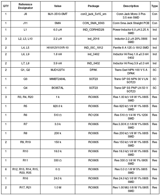
血压监视仪(BPM)参考设计材料清单(BOM):


责任编辑:HanFeng
【免责声明】
1、本文内容、数据、图表等来源于网络引用或其他公开资料,版权归属原作者、原发表出处。若版权所有方对本文的引用持有异议,请联系拍明芯城(marketing@iczoom.com),本方将及时处理。
2、本文的引用仅供读者交流学习使用,不涉及商业目的。
3、本文内容仅代表作者观点,拍明芯城不对内容的准确性、可靠性或完整性提供明示或暗示的保证。读者阅读本文后做出的决定或行为,是基于自主意愿和独立判断做出的,请读者明确相关结果。
4、如需转载本方拥有版权的文章,请联系拍明芯城(marketing@iczoom.com)注明“转载原因”。未经允许私自转载拍明芯城将保留追究其法律责任的权利。
拍明芯城拥有对此声明的最终解释权。
相关资讯
:
基于MC33771主控芯片的新能源锂电池管理系统解决方案

AMIC110 32位Sitara ARM MCU开发方案

基于AMIC110多协议可编程工业通信处理器的32位Sitara ARM MCU开发方案

基于展讯SC9820超低成本LTE芯片平台的儿童智能手表解决方案

基于TI公司的AM437x双照相机参考设计

基于MTK6580芯片的W2智能手表解决方案


 2012- 2022 拍明芯城ICZOOM.com 版权所有 客服热线:400-693-8369 (9:00-18:00)


