Freescale MPC8308无线通信参考设计方案
 85
85
 拍明
拍明
原标题:Freescale MPC8308无线通信参考设计方案
freescale公司的MPC8308是集成了 DDR2, eSDHC, PCI Express, eTSEC, USB, 和IEEE® 1588 的低功耗的PowerQUICC II Pro处理器,采用e300内核,具有更高的MIPS/MHZ性能,.处理器工作在266, 333和400 MHz ,具有1.92 DMIPS/ MHz性能,主要用在WLAN无线接入点,无线家庭基站,智能电网家庭网关,数据集中器,工业控制和工厂自动化.本文介绍了MPC8308处理器亮点,主要特性和优势,方框图以及MPC8308-RDB参考设计平台主要特性,方框图和电路图.
The MPC8308 is a cost-effective, lowpower, highly integrated PowerQUICCprocessor designed to address the requirements of networking applications such as smart grid home energy gateways, data concentrators, wireless LAN access points, wireless femto base stations and industrial applications such as industrial control and factory automation. It extends the PowerQUICC II Pro family by balancing the higher MIPS/MHz performance provided by the e300 core with low power consumption at a very aggressive price.
For networking applications, the Gigabit Ethernet MACs support connectivity to the wired network while the PCI Express® and SDIO interfaces can offer connectivity to wireless LAN or 3G and 4G modem devices. The MPC8308 processor features integrated IEEE for applications such as time-sensitive telecommunications services, industrial network switches, powerline networks and test/measurement devices. All of these applications will be fully enabled with the MPC8308 processor and the low-cost evaluation board with optimized Linux and drivers. Freescale also works with thirdparty partners to enable application software for end user interfaces.
Core Complex
The MPC8308 processor incorporates the e300c3 (603e core compatible) core at 266, 333 and 400 MHz with 1.92 DMIPS/ MHz. The core, built on Power Architecture® technology, includes dual integer units as well as a modified multiply instruction.
These architectural enhancements enable more efficient operations to be executed in parallel, resulting in a significant performance improvement. The e300 core complex also includes 16 KB each of L1 instruction and data caches and on-chip memory management units (MMUs) with dual integer units and SP/DP FPU.
Cost-Effective Package
The MPC8308 processor is designed with a very low-cost 473-pin MAPBGA package at 0.8 mm pitch and 19 mm x 19 mm dimension. This smaller package dimension is suitable for small-footprint applications in single-board computing and other embedded networking applications.
Cost-Effective Reference Design Board
The MPC8308-RDB (reference design board) is available to customers for US$299. The kit includes Linux drivers to support all peripherals, along with a free six-month evaluation license for CodeWarrior™ development tools.
MPC8308处理器亮点:

MPC8308主要特性和优势:

MPC8308应用:


图1.MPC8308方框图
MPC8308-RDB参考设计平台
The MPC8308-RDB reference platform is ideal for hardware and software development for embedded applications, including consumer printers, wireless access points, industrial control and factory automation equipment.It leverages the low-cost MPC8308 PowerQUICC® II Pro communications processor, built on Power Architecture® technology, which is designed to meet the requirements of several low-end embedded networking applications with high-speed peripherals while striving for low power consumption and a small-footprint package design. The MPC8308-RDB integrates leading-edge external components: 5 x Gigabit Ethernet ports, 1 x USB 2.0, x1 mini PCI Express® connector and an SD/MMC card interface. The MPC8308 microprocessor supports dual 10/100/1000 Mbps Ethernet controllers, single-lane PCI Express, USB 2.0 controller, enhanced SDHC controller for SD memory interface, dual universal asynchronous receiver/transmitter (DUART), serial peripherals, general-purpose I/O and system timers. This high level of integration in the MPC8308 processor helps to lower overall system costs, improve performance and simplify board design. The highspeed peripheral mix, combined with cost effectiveness, makes the MPC8308 processor a unique offering in the marketplace.
The MPC8308-RDB incorporates a preinstalled board support package (BSP) containing a boot loader (u-boot)—a generic Power Architecture technology system based on the Linux® kernel. The u-boot and Linux kernel reside in the on-board flash memory and launch when the board is powered up.
The MPC8308-RDB BSP takes advantage of the Linux Target Image Builder (LTIB)—a suite of tools that leverages existing open source configuration scripts and source code packages combining them all into a single BSP generation bundle. The source code packages, include boot loaders and Linux kernel sources, as well as many user-space source code packages, to build a complete BSP. The LTIB also provides compiler packages required to build the BSP. Freescale developers use the LTIB to create BSPs for a multitude of Freescale development markets.
The LTIB leverages as many BSP elements as possible for all Freescale markets supported, while offering the flexibility necessary to customize components that require platformspecific modifications.
Many third-party applications are available for the MPC8308-RDB. They are typically built on top of the BSP delivered by Freescale and can be installed on the hard disk.
MPC8308-RDB参考设计主要特性:
• CPU: Freescale MPC8308 running at 400/133 MHz; CPU/coherent system bus (CSB)
• Memory subsystem:
— 128 MByte unbuffered DDR2 SDRAM discrete devices
— 8 MByte NOR flash single-chip memory
— 32 MByte NAND flash memory
— 256 Kbit M24256 serial EEPROM
• Interfaces:
— 10/100/1000 BaseT Ethernet ports:
– eTSEC1, RGMII: one 10/100/1000 BaseT RJ-45 interface using Realtek™ RTL8211B single port 10/100/1000 BaseT PHY
– eTSEC2, RGMII: five 10/100/1000 BaseT RJ-45 interfaces using Vitesse™ VSC7385 5-port L2 Gigabit Ethernet switch
— USB 2.0 port:
– High-speed host/device/OTG USB interface using external ULPI PHY interface by SMSC USB3300 USB PHY
— PCI Express:
– One mini PCI Express connector supporting half and full size mini PCI Express card
— eSDHC port:
– One SD card connector
— Dual UART ports:
– DUART interface: supports two UARTs up to 115200 bps for console display
— I2C
– I2C connected to DallasTM DS1339 RTC with battery holder and AtmelTM AT24C08 Serial EEPROM
• Freescale MC9S08QG8 MCU (20-MHz HCS08 CPU) for fan control and soft start
— Support for Low Power / Wake on LAN. This can be MCU controlled or logic
• Board Connectors:
— 4 pins Power Jack connector
— Dual RS-232C connectors
— JTAG / COP for debugging
— IEEE® Std. 1588™ signals for test and measurement
— 8 pins SPI header for future expansion
• Form factor:

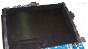
图2.MPC8308-RDB参考设计板外形图

图3.MPC8308-RDB参考设计方框图
责任编辑:HanFeng
【免责声明】
1、本文内容、数据、图表等来源于网络引用或其他公开资料,版权归属原作者、原发表出处。若版权所有方对本文的引用持有异议,请联系拍明芯城(marketing@iczoom.com),本方将及时处理。
2、本文的引用仅供读者交流学习使用,不涉及商业目的。
3、本文内容仅代表作者观点,拍明芯城不对内容的准确性、可靠性或完整性提供明示或暗示的保证。读者阅读本文后做出的决定或行为,是基于自主意愿和独立判断做出的,请读者明确相关结果。
4、如需转载本方拥有版权的文章,请联系拍明芯城(marketing@iczoom.com)注明“转载原因”。未经允许私自转载拍明芯城将保留追究其法律责任的权利。
拍明芯城拥有对此声明的最终解释权。


 产品分类
产品分类




 2012- 2022 拍明芯城ICZOOM.com 版权所有 客服热线:400-693-8369 (9:00-18:00)


