TI RM48Lx30安全系统MCU解决方案
 81
81
 拍明
拍明
原标题:TI RM48Lx30安全系统MCU解决方案
TI公司的RM48Lx30是高性能安全系统用的微控制器(MCU),它的安全架构包括两个步调一致的CPU,CPU和存储器内置自测(BIST)逻辑,闪存和数据SRAM的ECC,效率高达1.6 DMIPS/MHz的ARM® Cortex™-R4F浮点CPU,并可配置到在200MHz运行,提供高达320DMIPS,支持little-endian [LE32]格式,主要用在工业安全系统如工业自动化,安全PLC,电源产生和分布,电梯以及医疗电子如呼吸机, 心脏除颤器, 输液泵和胰岛素泵, 放射疗法和手术机器人等.本文介绍了RM48Lx30主要特性, 功能方框图和RM48 Hercules™ ARM® Safety MCU开发套件(HDK)主要特性,方框图与电路图.
The RM48Lx30 is a high performance microcontroller family for safety systems. The safety architecture includes Dual CPUs in lockstep, CPU and Memory Built-In Self Test (BIST) logic, ECC on both the Flash and the data SRAM, parity on peripheral memories, and loop back capability on peripheral IOs.
The RM48Lx30 integrates the ARM® Cortex™-R4F Floating Point CPU which offers an efficient 1.6 DMIPS/MHz, and has configurations which can run up to 200MHz providing up to 320 DMIPS. The device supports the little-endian [LE32] format.
The RM48Lx30 has up to 3MB integrated Flash and up to 256KB data RAM configurations with single bit error correction and double bit error detection. The flash memory on this device is a nonvolatile, electrically erasable and programmable memory implemented with a 64-bit-wide data bus interface. The flash operates on a 3.3V supply input (same level as I/O supply) for all read, program and erase operations. When in pipeline mode, the flash operates with a system clock frequency of up to 200MHz.
The SRAM supports single-cycle read/write accesses in byte, halfword, and word modes.
The RM48Lx30 device features peripherals for real-time control-based applications, including two Next Generation High End Timer (N2HET) timing coprocessors with up to 44 total IO terminals and a 12-bit Analog-to-Digital converter supporting up to 24 inputs.
The N2HET is an advanced intelligent timer that provides sophisticated timing functions for real-time applications. The timer is software-controlled, using a reduced instruction set, with a specialized timer micromachine and an attached I/O port. The N2HET can be used for pulse width modulated outputs, capture or compare inputs, or general-purpose I/O. It is especially well suited for applications requiring multiple sensor information and drive actuators with complex and accurate time pulses. A High End Timer Transfer Unit (HET-TU) can perform DMA type transactions to transfer N2HET data to or from main memory. A Memory Protection Unit (MPU) is built into the HET-TU.
The device has two 12-bit-resolution MibADCs with 24 total channels and 64 words of parity protected buffer RAM each. The MibADC channels can be converted individually or can be grouped by software for sequential conversion sequences. Sixteen channels are shared between the two MibADCs. There are three separate groupings. Each sequence can be converted once when triggered or configured for continuous conversion mode.
The device has multiple communication interfaces: three MibSPIs, up to two SPIs, one LIN, one SCI, three DCANs, one I2C. The SPI provides a convenient method of serial interaction for high-speed communications between similar shift-register type devices. The LIN supports the Local Interconnect standard 2.0 and can be used as a UART in full-duplex mode using the standard Non-Return-to-Zero (NRZ) format. The DCAN supports the CAN 2.0B protocol standard and uses a serial, multimaster communication protocol that efficiently supports distributed real-time control with robust communication rates of up to 1 megabit per second (Mbps). The DCAN is ideal for applications operating in noisy and harsh environments (e.g., automotive and industrial fields) that require reliable serial communication or multiplexed wiring.
The I2C module is a multi-master communication module providing an interface between the microcontroller and an I2C compatible device via the I2C serial bus. The I2C supports both 100 Kbps and 400 Kbps speeds.
The frequency-modulated phase-locked loop (FMPLL) clock module is used to multiply the external frequency reference to a higher frequency for internal use. The FMPLL provides one of the seven possible clock source inputs to the global clock module (GCM). The GCM module manages the mapping between the available clock sources and the device clock domains.
The device also has an external clock prescaler (ECP) module that when enabled, outputs a continuous external clock on the ECLK pin/ball. The ECLK frequency is a user-programmable ratio of the peripheral interface clock (VCLK) frequency. This low frequency output can be monitored externally as an indicator of the device operating frequency.
The Direct Memory Access Controller (DMA) has 16 channels, 32 control packets and parity protection on its memory. A Memory Protection Unit (MPU) is built into the DMA to protect memory against erroneous transfers.
The Error Signaling Module (ESM) monitors all device errors and determines whether an interrupt or external Error pin/ball is triggered when a fault is detected. The nERROR can be monitored externally as an indicator of a fault condition in the microcontroller.
The External Memory Interface (EMIF) provides a memory extension to asynchronous and synchronous memories or other slave devices.
Several interfaces are implemented to enhance the debugging capabilities of application code. In addition to the built in ARM Cortex™-R4F CoreSight™ debug features. An External Trace Macrocell (ETM) provides instruction and data trace of program execution. For instrumentation purposes, a RAM Trace Port Module (RTP) is implemented to support high-speed tracing of RAM and peripheral accesses by the CPU or any other master. A Data Modification Module (DMM) gives the ability to write external data into the device memory. Both the RTP and DMM have no or only minimum impact on the program execution time of the application code. A Parameter Overlay Module (POM) can re-route Flash accesses to internal memory or to the EMIF, thus avoiding the re-programming steps necessary for parameter updates in Flash.
With integrated safety features and a wide choice of communication and control peripherals, the RM48Lx30 is an ideal solution for high performance real time control applications with safety critical requirements.
RM48Lx30主要特性:
High-Performance Microcontroller for Safety Critical Applications
Dual CPU’s running in lockstep
ECC on flash and RAM interfaces
Built-In Self Test for CPU and on-chip RAMs
Error Signaling Module with Error Pin
Voltage and Clock Monitoring
ARM® Cortex™ - R4F 32-bit RISC CPU
Efficient 1.6DMIPS/MHz with 8-stage pipeline
Floating-Point Unit with Single/Double Precision
12-Region Memory Protection Unit
Open Architecture with 3rd Party Support
Operating Conditions
Up to 200MHz System Clock
Core Supply Voltage (VCC): 1.2V nominal
I/O Supply Voltage (VCCIO): 3.3V nominal
Integrated Memory
Up to 3MB Program Flash with ECC
Up to 256KB RAM with ECC
64KB Flash for emulated EEPROM
16- bit External Memory Interface
RM48Lx30应用:
Industrial Safety Applications
Industrial Automation
Safe PLC’s (Programmable Logic Controllers)
Power Generation and Distribution
Turbines and Windmills
Elevators and Escalators
Medical Applications
Ventilators
Defibrillators
Infusion and Insulin pumps
Radiation therapy
Robotic surgery

图1.RM48Lx30功能方框图
RM48 Hercules™ ARM® Safety MCU开发套件(HDK)
The RM48 Hercules Development Kit is ideal for getting started on development with the Hercules platform of safety microcontrollers. The development board features RJ45 10/100 Ethernet, USB-A Host, and USB-B Device Interfaces along with an on board XDS100v2 JTAG emulator and access to all peripheral pins. The kit is comprised of a development board, a DC power supply, a mini-B USB cable, an Ethernet cable and a software installation DVD that includes Code Composer Studio IDE, HALCoGen, nowFlash, HET IDE, demo software and code examples.
RM48开发套件(HDK)主要特性:
• A Texas Instruments RM48L950 337-pin BGA microcontroller
• On board USB XDS100v2 JTAG emulator
• ARM 20-pin JTAG debug header for external JTAG emulator
• External emulator detection circuit
• 10/100 Mbps Ethernet interface
• One USB host, and one USB device
• Two DCAN Transceivers and screw terminal blocks
• One ambient light sensor
• One ambient temperature sensor
• SCI accessible through a USB Virtual Port (VCP)
• One 8MB SDRAM
• Eight user programmable LEDs (2 tri-color LEDs, and 6 white LEDs)
• One user programmable pushbutton
• Three expansion connectors for hardware prototyping and daughter card use
• Reset pushbuttons (nPOR and nRST)
• One SD card slot (SPI mode)
• Embedded trace macrocell (ETM) debug interface via MIPI connector
• Configurable pin mux options
• 5V and 3.3V ADC option jumper (configured 5V by default)
• Current measurement capability for 3.3V IO, 1.2V Core, 1.2V PLL, 3.3V or 5V ADC, and 3.3V VCCP.
• Power supply supporting 5V to 12V DC input
RM48开发套件(HDK)包括:
RM48L950 Development board
CCStudio v4.x IDE: C/C++ Compiler/Linker/Debugger
HALCoGen Peripheral Driver Generation Tool
CCS and nowFlash Flash Programming Tools
HET IDE/Simulator/Assembler
GUI Demos with Project/Code Examples
Type A to mini B USB cable for using on board XDS100V2 JTAG emulator
Flashlight for light sensor demo

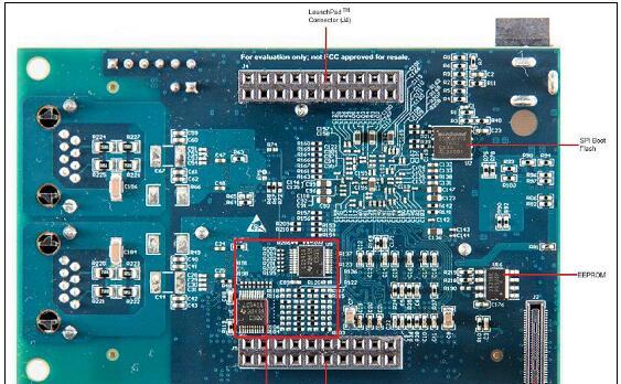
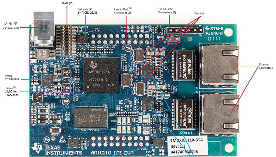
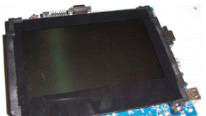
图2. RM48开发套件(HDK)外形图
责任编辑:HanFeng
【免责声明】
1、本文内容、数据、图表等来源于网络引用或其他公开资料,版权归属原作者、原发表出处。若版权所有方对本文的引用持有异议,请联系拍明芯城(marketing@iczoom.com),本方将及时处理。
2、本文的引用仅供读者交流学习使用,不涉及商业目的。
3、本文内容仅代表作者观点,拍明芯城不对内容的准确性、可靠性或完整性提供明示或暗示的保证。读者阅读本文后做出的决定或行为,是基于自主意愿和独立判断做出的,请读者明确相关结果。
4、如需转载本方拥有版权的文章,请联系拍明芯城(marketing@iczoom.com)注明“转载原因”。未经允许私自转载拍明芯城将保留追究其法律责任的权利。
拍明芯城拥有对此声明的最终解释权。


 产品分类
产品分类




 2012- 2022 拍明芯城ICZOOM.com 版权所有 客服热线:400-693-8369 (9:00-18:00)


