


 产品分类
产品分类
Renesas SH7264音频设备开发方案
 58
58
 拍明
拍明
原标题:Renesas SH7264音频设备开发方案
Renesas公司的SH7264是SH7260系列控制器, SH2A-FPU 32位CPU核,最大工作频率144MHz,具有极好的信号处理性能和ROM代码效率,使得音频应用如MP3, WMA或 AAC数据格式的压缩和解压更快,从而降低了程度的大小.主要用在汽车音频,HDD音频和网络音频,汽车图像仪表盘和汽车信息显示以及工业设备如定序器,机器人等.本文介绍了SH7264主要性能指标,方框图, 入门开发板主要指标,方框图和电路图,主要元件布局图以及音频DJ设备系统方框图.
Renesas Electronics had earlier launched the SH7260 Series of microcontrollers, built around the SH2A-FPU 32-bit CPU core with superb real time processing capability, as a solution for the digital audio field. The SH7262 and SH7264 belong to the SH7260 Series of microcontrollers, and the maximum operating frequency of 144 MHz enables faster operation in applications such as equipment control or digital audio signal processing. This combination of excellent signal processing performance and ROM code efficiency means that compression and decompression of audio data in formats required by digital audio applications, such as MP3, WMA, or AAC (Advanced Audio Coding), is performed more quickly and program sizes are reduced. Thanks to the newly added large-capacity SRAM, not only processing tasks related to equipment control and digital audio, but also video display capabilities can be implemented on as ingle chip. An ample 1 Mbyte or 640-Kbyte of on-chip SRAM is provided for video display use. It can be configured as a frame buffer to store video data temporarily, which is necessary when implementing graphical display capabilities. The generous SRAM capacity means that it is possible to use a TFTLCD panel display up to WQVGA size (480 × 240 pixels) without the need for external SDRAM as video memory.
The SH7262 and SH7264 provide a new video display controller and digital video input pins for use with graphical and video display applications. Digital RGB output pins allow output of images or video in RGB565 format at up to WQVGA size (480 × 240 pixels).
This reduces the total number of devices required and helps lower both the cost and the power consumption of the system.
This LSI is a single-chip RISC (reduced instruction set computer) microcontroller that includes a Renesas-original RISC CPU as its core, and the peripheral functions required to configure a system.
The CPU in this LSI is an SH-2A CPU, which provides upward compatibility for SH-1, SH-2, and SH-2E CPUs at object code level. It has a RISC-type instruction set, superscalar architecture, and Harvard architecture, for superior rates of instruction execution. In addition, the 32-bit internal-bus architecture that is independent from the direct memory access controller enhances data processing power. This CPU brings the user the ability to set up high-performance systems with strong functionality at less expense than was achievable with previous microcontrollers, and is even able to handle realtime control applications requiring high-speed characteristics.
This LSI has a floating-point unit and cache. In addition, this LSI includes on-chip peripheral functions necessary for system configuration, such as a 64-Kbyte RAM for high-speed operation, a 1-Mbyte or 640-Kbyte large-capacity RAM (32-Kbytes for 1-Mbyte and 320-Kbytes for 640-Kbyte versions are shared by the data-retention RAM), multi-function timer pulse unit 2, compare match timer, realtime clock, serial communication interface with FIFO, I2C bus interface 3, serial sound interface, serial I/O with FIFO, controller area network interface*2, IEBusTM*1 controller*2, Renesas SPDIF interface, CD-ROM decoder , A/D converter, NAND flash memory controller, USB 2.0 host/function, video display controller 3, sampling rate converter, SD host interface, decompression unit, motor control PWM timer, and interrupt controller modules, and general I/O ports.
This LSI also provides an external memory access support function to enable direct connection to various memory devices or peripheral LSIs. These on-chip functions significantly reduce costs of designing and manufacturing application systems.
SH7264主要指标:
CPU
Renesas original SuperH architecture
Compatible with SH-1, SH-2, and SH-2E at object code level
32-bit internal data bus
Support of an abundant register-set
⎯Sixteen 32-bit general registers
⎯Four 32-bit control registers
⎯Four 32-bit system registers
⎯Register bank for high-speed response to interrupts
RISC-type instruction set (upward compatible with SH series)
⎯Instruction length: 16-bit fixed-length basic instructions for improved code efficiency and 32-bit instructions for high performance and usability
⎯Load/store architecture
⎯Delayed branch instructions
⎯Instruction set based on C language
Superscalar architecture to execute two instructions at one time including a floating-point unit
Instruction execution time: Up to two instructions/cycle
Address space: 4 Gbytes
Internal multiplier
Five-stage pipeline
Harvard architecture
Floating-point unit Floating-point co-processor included
Supports single-precision (32-bit) and double-precision (64-bit)
Supports data type and exceptions that conforms to IEEE754 standard
Two rounding modes: Round to nearest and round to zero
Two denormalization modes: Flush to zero
Floating-point registers
⎯Sixteen 32-bit floating-point registers (single-precision 16 words or double-precision 8 words)
⎯Two 32-bit floating-point system registers
Supports FMAC (multiplication and accumulation) instructions
Supports FDIV (division) and FSQRT (square root) instructions
Supports FLDI0/FLDI1 (load constant 0/1) instructions
Instruction execution time
⎯Latency (FMAC/FADD/FSUB/FMUL): Three cycles (singleprecision), eight cycles (double-precision)
⎯Pitch (FMAC/FADD/FSUB/FMUL): One cycle (single-precision), six cycles (double-precision)
Note: FMAC only supports single-precision
Five-stage pipeline
Cache memory Instruction cache: 8 Kbytes
Operand cache: 8 Kbytes
128-entry/way, 4-way set associative, 16-byte block length configuration each for the instruction cache and operand cache
Write-back, write-through, LRU replacement algorithm
Way lock function available (only for operand cache); ways 2 and 3 can be locked
Interrupt controller Seventeen external interrupt pins (NMI, IRQ7 to IRQ0, and PINT7 to
PINT0)
On-chip peripheral interrupts: Priority level set for each module
16 priority levels available
Register bank enabling fast register saving and restoring in interrupt processing
Bus state controller
Address space divided into seven areas (0 to 6), each a maximum of 64 Mbytes
The following features settable for each area independently
⎯Bus size (8 or 16 bits): Available sizes depend on the area.
⎯Number of access wait cycles (different wait cycles can be specified for read and write access cycles in some areas)
⎯Idle wait cycle insertion (between the same area access cycles or different area access cycles)
⎯Specifying the memory to be connected to each area enables direct connection to SRAM, SRAM with byte selection, SDRAM, and burst ROM (clocked synchronous or asynchronous). The address/data multiplexed I/O (MPX) interface are also available.
⎯PCMCIA interface
⎯Outputs a chip select signal (CS0 to CS6) according to the target area (CS assert or negate timing can be selected by software)
SDRAM refresh
Auto refresh or self refresh mode selectable
SDRAM burst access
Direct memory access controller
Sixteen channels; external requests are available for one of them in the SH7262 Group, and for two of them in the SH7264 Group.
Can be activated by on-chip peripheral modules
Burst mode and cycle steal mode
Intermittent mode available (16 and 64 cycles supported)
Transfer information can be automatically reloaded
Clock pulse generator Clock mode: Input clock can be selected from external input (EXTAL or USB_X1) or crystal resonator
Input clock can be multiplied by 12 (max.) by the internal PLL circuit
Three types of clocks generated:
⎯CPU clock: Maximum 144 MHz
⎯Bus clock: Maximum 72 MHz
⎯Peripheral clock: Maximum 36 MHz
Watchdog timer
On-chip one-channel watchdog timer
A counter overflow can reset the LSI
Power-down modes Four power-down modes provided to reduce the power consumption in this LSI
⎯Sleep mode
⎯Software standby mode
⎯Deep standby mode
⎯Module standby mode
Multi-function timer pulse unit 2
Maximum 16 lines of pulse inputs/outputs based on fix channels of 16-bit timers
18 output compare and input capture registers
Input capture function
Pulse output modes
Toggle, PWM, complementary PWM, and reset-synchronized PWM modes
Synchronization of multiple counters
Complementary PWM output mode
⎯Non-overlapping waveforms output for 3-phase inverter control
⎯Automatic dead time setting
⎯0% to 100% PWM duty value specifiable
⎯A/D converter start request delaying function
⎯Interrupt skipping at crest or trough
Reset-synchronized PWM mode
Three-phase PWM waveforms in positive and negative phases can be output with a required duty value
Phase counting mode
Two-phase encoder pulse counting available
Compare match timer
Two-channel 16-bit counters
Four types of clock can be selected (P/8, P/32, P/128, and P/512)
DMA transfer request or interrupt request can be issued when a compare match occurs
Realtime clock
Internal clock, calendar function, alarm function
Interrupts can be generated at intervals of 1/256 s by the 32.768-kHz on-chip crystal oscillator Serial communication interface with FIFO
Eight channels
Clocked synchronous or asynchronous mode selectable (SH7262: channels 0 to 2, SH7264: channels 0 to 3)
Simultaneous transmission and reception (full-duplex communication) supported
Dedicated baud rate generator
Separate 16-byte FIFO registers for transmission and reception
Modem control function (SH7262: channel 1, SH7264: channels 1 and 3, in asynchronous mode)
Renesas serial peripheral interface
Two channels
SPI operation
Master mode and slave mode selectable
Programmable bit length, clock polarity, and clock phase can be selected.
Consecutive transfers
MSB first/LSB first selectable
Maximum transfer rate: 36 Mbps
I2C bus interface 3
Three channels
Master mode and slave mode supported
Serial sound interface
Four-channel bidirectional serial transfer
Duplex communication (channel 0)
Support of various real audio formats
Support of master and slave functions
Generation of programmable word clock and bit clock
Multi-channel formats
Support of 8, 16, 18, 20, 22, 24, and 32-bit data formats
Support of eight-stage FIFO for transmission and reception
Serial I/O with FIFO
Support of 16-stage 32-bits FIFOs independently for transmission and reception
8-bit monaural/16-bit monaural/16-bit stereo audio input and output
Connectable to linear, audio, or A-Law or -Law CODEC chip
Support of master and slave functions
Controller area network
Note: This module is included or not depending on the product code.
Two channels
TTCAN level 1 supports for all channels
BOSCH 2.0B active compatible
Buffer size: transmit/receive 31, receive only 1
Two or more controller area network channels can be assigned to one bus to increase number of buffers with a granularity of 32 channels
31 Mailboxes for transmission or reception
IEBusTM controller
Note: This module is included or not depending on the product code.
IEBus protocol control (layer 2) supported
⎯Half-duplex asynchronous communications
⎯Multi-master system
⎯Broadcast communications function
⎯Selectable mode (three types) with different transfer speeds
On-chip buffers (dual port RAM) for data transmission and reception that enable up to 128 bytes of consecutive transmit/reception (maximum number of transfer bytes in mode 2)
Operating frequency
⎯12 MHz, 12.58 MHz
(1/2 divided clocks of P, AUDIO_X1, or AUDIO_X2.)
⎯18 MHz, 18.87 MHz
(1/3 divided clocks of P, AUDIO_X1, or AUDIO_X2.)
⎯24 MHz
(1/4 divided clocks of P, AUDIO_X1, or AUDIO_X2.)
⎯25.16 MHz (1/4 divided clocks of P)
⎯30 MHz, 31.45 MHz (1/5 divided clocks of P)
⎯36 MHz (1/6 divided clocks of P)
Renesas SPDIF interface
Support of IEC60958 standard (stereo and consumer use modes only)
Sampling frequencies of 32 kHz, 44.1 kHz, and 48 kHz
Audio word sizes of 16 to 24 bits per sample
Biphase mark encoding
Double buffered data
Parity encoded serial data
Simultaneous transmit and receive
Receiver autodetects IEC 61937 compressed mode data
CD-ROM decoder
Support of five formats: Mode 0, mode 1, mode 2, mode 2 form 1, and mode 2 form 2
Sync codes detection and protection (Protection: When a sync code is not detected, it is automatically inserted.)
Descrambling
ECC correction
⎯P, Q, PQ, and QP correction
⎯PQ or QP correction can be repeated up to three times
EDC check
Performed before and after ECC
Mode and form are automatically detected
Link sectors are automatically detected
Buffering data control
Buffering CD-ROM data including Sync code is transferred in specified format, after the data is descrambled, corrected by ECC, and checked by EDC.
NAND flash memory controller
Direct-connected memory interface with NAND-type flash memory
Read/write in sectors
Two types of transfer modes: Command access mode and sector access mode (512-byte data + 16-byte management code: with ECC)
Interrupt request and DMA transfer request
Supports flash memory requiring 5-byte addresses (2 Gbits and more) USB 2.0 host/function module
Conforms to the Universal Serial Bus Specification Revision 2.0
480-Mbps, 12-Mbps, and 1.5-Mbps transfer rates provided (host mode)
480-Mbps and 12-Mbps transfer rates provided (function mode)
On-chip 8-Kbyte RAM as communication buffers
Video display controller 3
Video input Input format: BT601, BT656 (NTSC/PAL)
Video recording Can be saved in RGB565 format, at 1/2 field rate.
Video processing
Video scaling: 1/2, 1/3, 1/4
Horizontal scaling: 1/2, 1/3, 2/3, 1/4 (Each scaling value can be multiplied by 6/7 for PAL.)
Adjustment of contrast and brightness
Graphic image 1 and 2 (two layers)
Input format: RGB565 (16 bits), RGB4444 (16 bits)
Overlap function
-blending window function: Mixes input image, layer 1, and layer 2 in a specified area according to the transmittance (fadein and face-out possible).
Chromakey function: Mixes images according to the specified RGB color and transmittance .
Dot a function: Mixes RGB4444-format graphic images according to the transmittance Output image
Resolution: VGA (640 480), WQVGA (480 240), QVGA (320 240), QVGA (240 320)
Format: RGB565 (16 bits)
Sampling rate converter
Data format: 32-bit stereo (16 bits each to L/R), 16-bit monaural for channel 0, and 16-bit monaural for channel 1
Input sampling rate: 8/11.025/12/16/22.05/24/32/44.1/48kHz (channel 0), 44.1kHz (channel 1)
Output sampling rate: 44.1/48 kHz (channel 0), 8/16 kHz (channel 1)
SD host interface
SD memory I/O card interface (1-/4-bits SD bus)
Error check function: CRC7 (command), CRC16 (data)
Interrupt requests
⎯Card access interrupt
⎯SDIO access interrupt
⎯Card detect interrupt
DMA transfer requests
⎯SD_BUF write
⎯SD_BUF read
Card detect function, write protect supported
Decompression unit
Input data
Data compressed with run-length encoding
Output data
RAW data
General I/O ports
SH7262: 89 I/Os, 6 inputs with open-drain outputs, and 4 inputs
SH7264: 115 I/Os, 6 inputs with open-drain outputs, and 8 inputs
Input or output can be selected for each bit
A/D converter
10-bit resolution
SH7262: four input channels, SH7264: eight input channels
A/D conversion request by the external trigger or timer trigger Motor control PWM
timer
Two 10-bit PWM channels, each with eight outputs User debugging interface
E10A emulator support
JTAG-standard pin assignment
On-chip RAM
64-Kbyte memory for high-speed operation (16 Kbytes 4)
1-Mbyte or 640-Kbyte large capacity memory for video display/recording and work (32-Kbytes for 1-Mbyte and 320-Kbytes for 640-Kbyte versions are used for data retention)
1-Mbyte version: 32-Kbyte memory for data retention (16 Kbytes 2)
640-Kbyte version: 320-Kbyte memory for data retention (16 Kbytes2, 128 Kbytes1, 160 Kbytes1)
Boot modes
Four boot modes
Boot mode 0: Booting from memory connected to CS0 area
Boot mode 1: Booting from a serial flash memory (high-speed communication)
Boot mode 2: Booting from a NAND flash memory
Boot mode 3: Booting from a serial flash memory (low-speed communication)
Power supply voltage
Vcc: 1.1 to 1.3 V
PVcc: 3.0 to 3.6 V
Packages
SH7262
176-pin QFP, 24-mm square, 0.5-mm pitch
JEITA package code: P-LQFP176-24 24-0.50
Renesas code: PLQP0176KB-A
SH7264
208-pin QFP, 28-mm square, 0.5-mm pitch JEITA package code: P-LQFP208-28 28-0.50
Renesas code: PLQP0208KB-A
SH7264主要应用:
Audio: car audio, HDD audio and Network audio.
Graphic dashboard, Vehicle information display.
Industrial equipment: sequencer, robot etc.
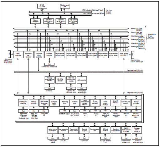
图1.SH7264方框图
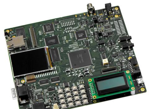
图2.SH7264入门板外形图
入门板主要指标:
Item
Specification
Microcontroller
R5S72643P144FPU
On-board Memory
Serial Flash (M25PX64): 64 Mbit
NAND Flash (K9NBG08U5M-PCB0): 8 Gbit
NOR Flash (S29GL512P-10T-AIR20): 512 Mbit
SDRAM (IS42S16320B-7TL): 64 MB
Input Clock
Main: 18 MHz
Sub: 32.768 kHz
LCD: 25.175 MHz
USB: 48 MHz
Video Decoder: 24.576 MHz
External DAC/ADC (for CODEC): 13 MHz
Ethernet (for PHY): 25 MHz
Potentiometer
Single-turn, 10 kΩ
LED
5 V Power indicator: blue x 1
3.3 V Power indicator: green x 1
User: yellow x 3
Switch
Reset x 1
User x 16
DC Power Jack
5 V Input
E10A-USB Header
14-pin box header
RS232 Serial Connector
9-pin DSUB
LCD Display Connector
14-pin socket
TFT-LCD Panel Connector
Hitatch 2.2' QVGA TFT: 39-pin (CN11)
Generic LCD: 30-pin (JP12)
USB Connector
Socket-A & Mini-B
CAN Connector
2.54 mm pitch, 3-pin (CAN Bus line x 2, Ground x 1)
Ethernet Connector
SD Card Connector
Reverse Type
Audio Jack
Headphone & Speaker
Video Jack
Compsite & Separate
VGA Connector
DB15H
Microcontroller Pin Header
56-pin (JP15), 32-pin (JP16)
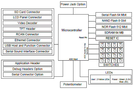
图3.SH7264入门板方框图
音频DJ设备
DJ equipment is a device for playing back, mixing, and scratching music from CD and audio data as if they were from a vinyl record. DJ equipment is mainly made up of two DJ players and one DJ mixer. Although mainly used in North America and Europe until now, recently sales numbers of DJ equipment are increasing in emerging countries such as Russia and Brazil. In addition, although mostly used by businesses such as discos, due to the appearance of low-cost products private users are also increasing in number.
Renesas Electronics simplifies the development of DJ equipment with SH726x 32-bit RISC microcontrollers with functions necessary for DJ equipment built-in and a lineup of motor drivers, power supply ICs, various standard ICs, opto-electronics devices, and so on.
SH726x microcontrollers are built around the SH2A-FPU high-performance CPU core and integrate on-chip peripheral functions, such as an SD memory card interface, a NAND flash memory controller, USB, a CD-ROM decoder, and a serial sound interface.
In addition, a variety of middleware products, such as an MP3 encoder/decoder, are available, allowing for flexible extension of functions and reducing the time required for system development.
责任编辑:HanFeng
【免责声明】
1、本文内容、数据、图表等来源于网络引用或其他公开资料,版权归属原作者、原发表出处。若版权所有方对本文的引用持有异议,请联系拍明芯城(marketing@iczoom.com),本方将及时处理。
2、本文的引用仅供读者交流学习使用,不涉及商业目的。
3、本文内容仅代表作者观点,拍明芯城不对内容的准确性、可靠性或完整性提供明示或暗示的保证。读者阅读本文后做出的决定或行为,是基于自主意愿和独立判断做出的,请读者明确相关结果。
4、如需转载本方拥有版权的文章,请联系拍明芯城(marketing@iczoom.com)注明“转载原因”。未经允许私自转载拍明芯城将保留追究其法律责任的权利。
拍明芯城拥有对此声明的最终解释权。
相关资讯
:
基于MC33771主控芯片的新能源锂电池管理系统解决方案

AMIC110 32位Sitara ARM MCU开发方案

基于AMIC110多协议可编程工业通信处理器的32位Sitara ARM MCU开发方案

基于展讯SC9820超低成本LTE芯片平台的儿童智能手表解决方案

基于TI公司的AM437x双照相机参考设计

基于MTK6580芯片的W2智能手表解决方案


 2012- 2022 拍明芯城ICZOOM.com 版权所有 客服热线:400-693-8369 (9:00-18:00)


