Freescale S08MM128医疗设备开发方案
 74
74
 拍明
拍明
原标题:Freescale S08MM128医疗设备开发方案
freescale公司的 9S08MM128/64/32是Flexis 8位MCU,具有超低功耗,USB连接和支持图像显示以及无与伦比的测量精度。S08MM128工作电压2.4V时的CPU速率高达48MHz,支持多达 33条中断/重置源,128KB双阵列闪存读/编/除功能,12KB RAM,并具有安全电路,防止未许可接入RAM和闪存,并有多种外设接口,主要用在工业,仪表,医疗/保健如血压计,心率监视器,血糖仪,ECG等。本文介绍了S08MM128主要特性,方框图,以及开发工具TWR-S08MM128-KIT主要特性,方框图以及电路图。
The 9S08MM128/64/32 provides ultra-low-power operation, USB connectivity, graphic display support and unparalleled measurement accuracy, all in a single 8-bit microcontroller, allowing device designers to create more fully featured products at a lower cost.
The 9S08MM128/64/32 is ideal for medical applications or any other application requiring a significant amount of precision analog such as instrumentation and industrial control. The 9S08MM128/64/32 is part of the Freescale Flexis™ microcontroller series.
S08MM128主要特性:
8-Bit HCS08 Central Processor Unit (CPU)
– Up to 48-MHz CPU above 2.4 V, 40 MHz CPU above 2.1 V, and
20 MHz CPU above 1.8 V across temperature of -40°C to 105°C
– HCS08 instruction set with added BGND instruction
– Support for up to 33 interrupt/reset sources
On-Chip Memory
– 128 K Dual Array Flash read/program/erase over full operating voltage and temperature
– 12 KB Random-access memory (RAM)
– Security circuitry to prevent unauthorized access to RAM and Flash
Power-Saving Modes
– Two ultra-low power stop modes. Peripheral clock enable register can disable clocks to unused modules to reduce currents
– Time of Day (TOD) — Ultra-low power 1/4 sec counter with up to 64s timeout.
– Ultra-low power external oscillator that can be used in stop modes to provide accurate clock source to the TOD. 6 usec typical wake up time from stop3 mode
Clock Source Options
– Oscillator (XOSC1) — Loop-control Pierce oscillator; 32.768 kHz crystal or ceramic resonator dedicated for TOD operation.
– Oscillator (XOSC2) — for high frequency crystal input for MCG reference to be used for system clock and USB operations.
– Multipurpose Clock Generator (MCG) — PLL and FLL; precision trimming of internal reference allows 0.2% resolution and 2% deviation over temperature and voltage; supports CPU frequencies from 4 kHz to 48 MHz.
System Protection
– Watchdog computer operating properly (COP) reset Watchdog computer operating properly (COP) reset with option to run from dedicated 1-kHz internal clock source or bus clock
– Low-voltage detection with reset or interrupt; selectable trip points; separate low-voltage warning with optional interrupt; selectable trip points
– Illegal opcode and illegal address detection with reset
– Flash block protection for each array to prevent accidental write/erasure
– Hardware CRC to support fast cyclic redundancy checks
Development Support
– Single-wire background debug interface
– Real-time debug with 6 hardware breakpoints (4 PC, 1 address and 1 data) Breakpoint capability to allow single breakpoint setting during in-circuit debugging
– On-chip in-circuit emulator (ICE) debug module containing 3 comparators and 9 trigger modes
Peripherals
– CMT— Carrier Modulator timer for remote control communications. Carrier generator, modulator and driver for dedicated infrared out. Can be used as an output compare timer.
– IIC— Up to 100 kbps with maximum bus loading; Multi-master operation; Programmable slave address; Interrupt driven byte-by-byte data transfer; supports broadcast mode and 11-bit addressing
– PRACMP — Analog comparator with selectable interrupt; compare option to programmable internal reference voltage; operation in stop3
– SCI — Two serial communications interfaces with optional 13-bit break; option to connect Rx input to PRACMP output on SCI1 and SCI2; High current drive on Tx on SCI1 and SCI2; wake-up from stop3 on Rx edge
– SPI1— Serial peripheral interface (SPI) with 64-bit FIFO buffer; 16-bit or 8-bit data transfers; full-duplex or single-wire bidirectional; double-buffered transmit and receive; master or slave mode; MSB-first or LSB-first shifting
– SPI2— Serial peripheral interface with full-duplex or single-wire bidirectional; Double-buffered transmit and receive; Master or Slave mode; MSB-first or LSB-first shifting
– TPM — Two 4-channel Timer/PWM Module; Selectable input capture, output compare, or buffered edge- or center-aligned PWM on each channel; external clock input/pulse accumulator
– USB — Supports USB in full-speed device configuration. On-chip transceiver and 3.3V regulator help save system cost, fully compliant with USB Specification 2.0. Allows control, bulk, interrupt and isochronous transfers. Not available on MC9S08MM32A devices.
– ADC16 — 16-bit Successive approximation ADC with up to 4 dedicated differential channels and 8 single-ended channels; range compare function; 1.7 mV/C temperature sensor; internal bandgap reference channel; operation in stop3; fully functional from 3.6V to 1.8V, Configurable hardware trigger for 8 Channel select and result registers
– PDB — Programmable delay block with 16-bit counter and modulus and prescale to set reference clock to bus divided by 1 to bus divided by 2048; 8 trigger outputs for ADC16 module provides periodic coordination of ADC sampling sequence with sequence completion interrupt; Back-to-Back mode and Timed mode
– DAC— 12-bit resolution; 16-word data buffers with configurable watermark.
– OPAMP — Two flexible operational amplifiers configurable for general operations; Low offset and temperature drift.
– TRIAMP — Two trans-impedance amplifiers dedicated for converting current inputs into voltages.
Input/Output
– Up to 47 GPIOs and 2 output-only pin and 1 input-only pin.
– Voltage Reference output (VREFO).
– Dedicated infrared output pin (IRO) with high current sink capability.
– Up to 16 KBI pins with selectable polarity.
Package Options
– 81-MBGA 10x10 mm
– 80-LQFP 12x12 mm
64-LQFP 10x10 mm
S08MM128目标应用:
Industrial
Instrumentation
Medical/Healthcare
Blood Pressure Monitors
Heart Rate Monitors
Pulse Oximetry
Ultrasound
Telehealth System
Hospital Admission Machine
Blood Glucose Monitors (Glucometers)
Electrocardiograph (ECG)
Anesthesia Unit Monitor
Vital Signs Monitors
Defibrillators

图1。MC9S08MM128系列方框图
TWR-S08MM128-KIT医疗设备开发工具
The TWR-S08MM128-KIT is a medical-oriented development tool for the 9S08MM128 microcontroller.
This kit is part of the Freescale Tower System, a modular, reconfigurable development platform that allows designers to get to market faster with packaged evaluation boards, tools and runtime software.
The kit includes the MED-EKG which is an electrocardiograph sensor for medical applications development. The 9S08MM microcontroller module is designed to be a standalone debug tool and can also be purchased separately from the kit, part number TWR-S08MM128.
TWR-S08MM128-KIT医疗设备开发工具主要特性:
Freescale Tower System compliant
Integrated open-source BDM debugging tool
Small form factor (59mm x 90mm)
Supports external communications interfaces
Includes power regulation circuitry with standardized bus
Two 80-pin connectors on the outside to support debugging or expansion to LCD module RS232, RS485, CAN , USB
Open connector for MED-EKG development board
Low power
TWR-S08MM128-KIT医疗设备开发工具包括:
TWR-S08MM128 - 8-bit module that features the 9S08MM128
TWR-SER - Serial module that features Ethernet, USB, RS232/485 and CAN
TWR-ELEV - Two elevator boards that provide structural integrity, communications interfaces, power regulation circuitry with standardized bus
Necessary cables
MED-EKG - Electrocardiograph sensor to develop medical applications with Flexis MM Family
An interactive DVD with lab tutorials, software, training and collateral
A printed guide on how to quickly get started using the development kit

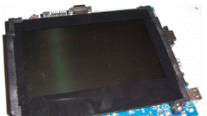
图2。TWR-S08MM128-KIT外形图

图3。TWR-S08MM128-KIT方框图
责任编辑:HanFeng
【免责声明】
1、本文内容、数据、图表等来源于网络引用或其他公开资料,版权归属原作者、原发表出处。若版权所有方对本文的引用持有异议,请联系拍明芯城(marketing@iczoom.com),本方将及时处理。
2、本文的引用仅供读者交流学习使用,不涉及商业目的。
3、本文内容仅代表作者观点,拍明芯城不对内容的准确性、可靠性或完整性提供明示或暗示的保证。读者阅读本文后做出的决定或行为,是基于自主意愿和独立判断做出的,请读者明确相关结果。
4、如需转载本方拥有版权的文章,请联系拍明芯城(marketing@iczoom.com)注明“转载原因”。未经允许私自转载拍明芯城将保留追究其法律责任的权利。
拍明芯城拥有对此声明的最终解释权。


 产品分类
产品分类



 2012- 2022 拍明芯城ICZOOM.com 版权所有 客服热线:400-693-8369 (9:00-18:00)


