


 产品分类
产品分类
ADI AD9277低成本低功耗医疗超声解决方案
 57
57
 拍明
拍明
原标题:ADI AD9277低成本低功耗医疗超声解决方案
ADI公司的AD9277是低成本低功耗小型容易使用的8路14位ADC,包括8路可变增益放大器(VGA)和低噪音放大器(LNA),抗混淆滤波器 (AAF)和14位10MSPS到50MSPS本世纪末ADC以及可编相位旋转的I/Q解调器,主要用在医疗图像和超声波图像以及汽车雷达.本文介绍了 AD9277主要特性和产品亮点,方框图, 超声波系统方框图以及AD9277评估板主要特性,评估板连接图,电路图,PCB布局图和材料清单.此外还介绍了ADI医疗超声解决方案方框图和信号链接图.
The AD9277 is designed for low cost, low power, small size, and ease of use. It contains eight channels of a variable gain amplifier (VGA) with a low noise preamplifier (LNA); an anti-aliasing filter (AAF); a 14-bit, 10 MSPS to 50 MSPS analog-to-digital converter (ADC); and an I/Q demodulator with programmable phase rotation.
Each channel features a variable gain range of 42 dB, a fully differ-ential signal path, an active input preamplifier termination, a maximum gain of up to 52 dB, and an ADC with a conversion rate of up to 50 MSPS. The channel is optimized for dynamic performance and low power in applications where a small package size is critical.
The LNA has a single-ended-to-differential gain that is selectable through the SPI. The LNA input noise is typically 0.75 nV/√Hz at a gain of 21.3 dB, and the combined input-referred noise of the entire channel is 0.85 nV/√Hz at maximum gain. Assuming a 15 MHz noise bandwidth (NBW) and a 21.3 dB LNA gain, the input SNR is roughly 92 dB. In CW Doppler mode, each LNA output drives an I/Q demodulator. Each demodulator has inde-pendently programmable phase rotation through the SPI with 16 phase settings.
The AD9277 requires a LVPECL-/CMOS-/LVDS-compatible sample rate clock for full performance operation. No external reference or driver components are required for many applications.
The ADC automatically multiplies the sample rate clock for the appropriate LVDS serial data rate. A data clock (DCO±) for capturing data on the output and a frame clock (FCO±) trigger for signaling a new output byte are provided.
Powering down individual channels is supported to increase battery life for portable applications. A standby mode option allows quick power-up for power cycling. In CW Doppler opera-tion, the VGA, AAF, and ADC are powered down. The power of the TGC path scales with selectable ADC speed power modes.
The ADC contains several features designed to maximize flexibility and minimize system cost, such as a programmable clock, data alignment, and programmable digital test pattern generation. The digital test patterns include built-in fixed patterns, built-in pseudo-random patterns, and custom user-defined test patterns entered via the serial port interface.
Fabricated in an advanced CMOS process, the AD9277 is available in a 16 mm × 16 mm, RoHS compliant, 100-lead TQFP. It is specified over the industrial temperature range of −40℃ to +85℃.
AD9277产品亮点:
Small Footprint. Eight channels are contained in a small, space-saving package. Full TGC path, ADC, and I/Q demodulator contained within a 100-lead, 16 mm × 16 mm TQFP.
Low Power. In TGC mode, low power of 207 mW per channel at 50 MSPS. In CW mode, ultralow power of 94 mW per channel.
Integrated High Dynamic Range I/Q Demodulator with Phase Rotation.
Ease of Use. A data clock output (DCO±) operates up to 480 MHz and supports double data rate (DDR) operation.
User Flexibility. Serial port interface (SPI) control offers a wide range of flexible features to meet specific system requirements.
Integrated Second-Order Antialiasing Filter. This filter is placed before the ADC and is programmable from 8 MHz to 18 MHz.
AD9277主要特性:
8 channels of LNA, VGA, AAF, ADC, and I/Q demodulator
Low noise preamplifier (LNA)
Input-referred noise: 0.75 nV/√Hz typical at 5 MHz (gain = 21.3 dB)
SPI-programmable gain: 15.6 dB/17.9 dB/21.3 dB
Single-ended input: VIN maximum = 733 mV p-p/ 550 mV p-p/367 mV p-p
Dual-mode active input impedance matching
Bandwidth (BW) > 100 MHz
Full-scale (FS) output: 4.4 V p-p differential
Variable gain amplifier (VGA)
Attenuator range: −42 dB to 0 dB
Postamp gain: 21 dB/24 dB/27 dB/30 dB
Linear-in-dB gain control
Antialiasing filter (AAF)
Programmable second-order LPF from 8 MHz to 18 MHz
Programmable HPF
Analog-to-digital converter (ADC)
14 bits at 10 MSPS to 50 MSPS
SNR: 73 dB
SFDR: 75 dB
Serial LVDS (ANSI-644, IEEE 1596.3 reduced range link)
Data and frame clock outputs
CW mode I/Q demodulator
Individual programmable phase rotation
Output dynamic range per channel >160 dBFS/√Hz
Low power: 207 mW per channel at 14 bits/50 MSPS (TGC), 94 mW per channel for CW Doppler
Flexible power-down modes
Overload recovery in <10 ns
Fast recovery from low power standby mode: <2 μs
100-lead TQFP_EP
AD9277应用:
Medical imaging/ultrasound
Automotive radar

图1. AD9277功能方框图

图2. 简化超声波系统方框图

图3. 简化超声波系统单路方框图
AD9277评估板
AD9277评估板主要特性:
Full featured evaluation board for the AD9276 and the AD9277
SPI and alternate clock options
Internal and external reference options
VisualAnalog and SPI Controller software interfaces
EQUIPMENT NEEDED
Analog signal source and antialiasing filter
2 switching power supplies (6.0 V, 2.5 A) CUI EPS060250UH-PHP-SZ, provided
Linear bench top dc voltage source (0 V to 1.6 V), not required for CW Doppler mode
PC running Windows® 98 (2nd edition), Windows 2000, Windows ME, or Windows XP
USB 2.0 port, recommended (USB 1.1 compatible)
AD9276 and AD9277 evaluation board
HSC-ADC-EVALCZ FPGA-based data capture kit
For CW Doppler mode: spectrum analyzer

图4. AD9276-65EBZ/AD9276-80KITZ/AD9277-50EB评估板和HSC-ADC-EVALCZ数据采集板外形图

图5. AD9277评估板连接框图
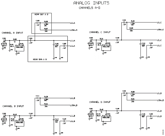
图6. AD9277评估板电路图(1)

图7. AD9277评估板电路图(2)

图8. AD9277评估板电路图(3)

图9. AD9277评估板电路图(4)

图10. AD9277评估板电路图(5)

图11. AD9277评估板电路图(6)
AD9277评估板材料清单:


ADI医疗超声解决方案
超声系统可以通过向人体发射声学能量,然后接收并处理回波,从而产生内部器官和结构的图像,绘制血液流动和组织运动图,以及提供高度精确的血流速度信息。
超声系统包含传感器、高压开关、高压发射电路、发射(Tx)/接收(Rx)开关、接收通道模拟前端(AFE)、波束形成器、波束形成后的数字信号处理电路、显示处理电路和外设。AFE包括低噪声放大器(LNA)、可变增益放大器(VGA)、抗混叠滤波器(AAF)和模数转换器(ADC)。针对不同应用,波束形成可以分为两类:数字波束形成和模拟波束形成。
医疗超声系统设计考虑和主要挑战
• AFE电路性能,如噪声性能、信噪比(SNR)和动态范围(DR)等,动态范围的典型要求如下:B模式70 dB,PWD(脉冲波多普勒)140 dB,CWD(连续波多普勒)160 dB。
• 发射电压——为提高信号穿透率以及进行谐波成像,需要很高的发射电压。声功率随着发射电压增大而提高,但发射声功率不能超过美国食品和药品管理局(FDA)等机构规定的安全要求限制。
• 波束形成器的复杂度——要获得高图像质量,就要求采用大量波束形成通道。复杂度增加进而导致功耗升高,并且需要更多成像通道来实施。
• 散热——随着设备向小型化发展,尤其是在还要提高图像质量的时候,散热问题显得非常重要。

图13.ADI医疗超声解决方案外形图

图14.ADI医疗超声解决方案方框图

图15.ADI医疗超声解决方案信号链接框图
责任编辑:HanFeng
【免责声明】
1、本文内容、数据、图表等来源于网络引用或其他公开资料,版权归属原作者、原发表出处。若版权所有方对本文的引用持有异议,请联系拍明芯城(marketing@iczoom.com),本方将及时处理。
2、本文的引用仅供读者交流学习使用,不涉及商业目的。
3、本文内容仅代表作者观点,拍明芯城不对内容的准确性、可靠性或完整性提供明示或暗示的保证。读者阅读本文后做出的决定或行为,是基于自主意愿和独立判断做出的,请读者明确相关结果。
4、如需转载本方拥有版权的文章,请联系拍明芯城(marketing@iczoom.com)注明“转载原因”。未经允许私自转载拍明芯城将保留追究其法律责任的权利。
拍明芯城拥有对此声明的最终解释权。
相关资讯
:
基于MC33771主控芯片的新能源锂电池管理系统解决方案

AMIC110 32位Sitara ARM MCU开发方案

基于AMIC110多协议可编程工业通信处理器的32位Sitara ARM MCU开发方案

基于展讯SC9820超低成本LTE芯片平台的儿童智能手表解决方案

基于TI公司的AM437x双照相机参考设计

基于MTK6580芯片的W2智能手表解决方案


 2012- 2022 拍明芯城ICZOOM.com 版权所有 客服热线:400-693-8369 (9:00-18:00)


