


 产品分类
产品分类
ADI AD5780 18位精度低噪音±10 V DC电压源解决方案
 70
70
 拍明
拍明
原标题:ADI AD5780 18位精度低噪音±10 V DC电压源解决方案
ADI公司的AD5780是真正18位线性低噪音精密的±10 V DC电压源,工作电压双极电压高达33V,采用正基准输入电压从5V到VDD-2.5V,而负基准输入电压从VSS+2.5V到0V,输出噪音8 nV/√Hz,长期稳定性为0.025 LSB,增益误差±0.018 ppm/℃,输出电压设定时间2.5 μs, 施密特触发器数字接口35MHz,1.8V兼容数字接口,主要用在医疗仪器,测试测量,工业控制,数据采集系统,数字增益和失调调整,电源控制等.本文介绍了AD57801产品亮点和主要特性, 功能框图和典型工作电路图以及评估板EVAL-AD5780主要特性,电路图,材料清单和PCB布局图.
The AD57801 is a true 18-bit, unbuffered voltage output DAC that operates from a bipolar supply of up to 33 V. The AD5780 accepts a positive reference input range of 5 V to VDD − 2.5 V and a negative reference input range of VSS + 2.5 V to 0 V. Both reference inputs are buffered on chip and external buffers are not required. The AD5780 offers a relative accuracy specifica-tion of ±1 LSB maximum range, and operation is guaranteed monotonic with a ±1 LSB DNL maximum range specification.
The part uses a versatile 3-wire serial interface that operates at clock rates of up to 35 MHz and is compatible with standard SPI, QSPI™, MICROWIRE™, and DSP interface standards. The part incorporates a power-on reset circuit that ensures that the DAC output powers up to 0 V in a known output impedance state and remains in this state until a valid write to the device takes place. The part provides an output clamp feature that places the output in a defined load state.
AD57801产品亮点:
True 18-bit accuracy.
Wide power supply range of up to ±16.5 V.
−40℃ to +125℃ operating temperature range.
Low 8 nV/√Hz noise.
Low ±0.018 ppm/℃ gain error temperature coefficient
AD57801主要特性:
True 18-bit voltage output DAC, ±1 LSB INL
8 nV/√Hz output noise spectral density
0.025 LSB long-term linearity error stability
±0.018 ppm/°C gain error temperature coefficient
2.5 μs output voltage settling time
3.5 nV-sec midscale glitch impulse
Integrated precision reference buffers
Operating temperature range: −40℃ to +125℃
4 mm × 5 mm LFCSP package
Wide power supply range of up to ±16.5 V
35 MHz Schmitt triggered digital interface
1.8 V-compatible digital interface
AD57801应用:
Medical instrumentation
Test and measurement
Industrial control
Scientific and aerospace instrumentation
Data acquisition systems
Digital gain and offset adjustment
Power supply control
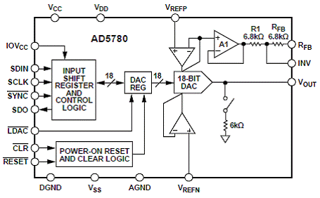
图1.AD57801功能框图
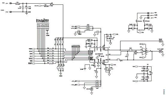
图2.AD57801典型工作电路图
AD57801评估板EVAL-AD5780
Evaluation Board for a 18-Bit Serial Input, Voltage Output DAC with Integrated Precision Reference Buffer Amplifiers
The EVAL-AD5780 is a full-featured evaluation board, designed to allow the user to easily evaluate all features of the AD5780 voltage output, 18-bit digital-to-analog converter (DAC). The AD5780 pins are accessible at on-board connectors for external connection. The board can be controlled by two means: via the on-board connector (J3), or via the system development platform connector (J4). The SDP board allows the evaluation board to be controlled through the USB port of a Windows® XP- (SP2 or later) or Vista-based (32-bit) PC using the AD5780 evaluation software.
评估板EVAL-AD5780主要特性:
Full-featured evaluation board for the AD5780
Link options
PC control in conjunction with Analog Devices, Inc., system development platform
PC software for control
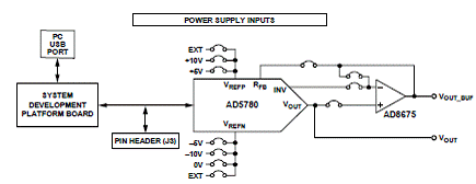
图3.评估板EVAL-AD5780框图
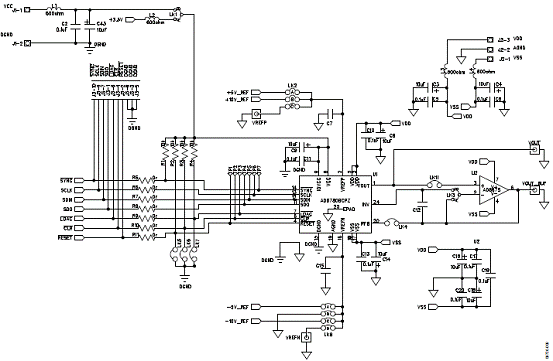
图4.评估板EVAL-AD5780电路图:AD5780
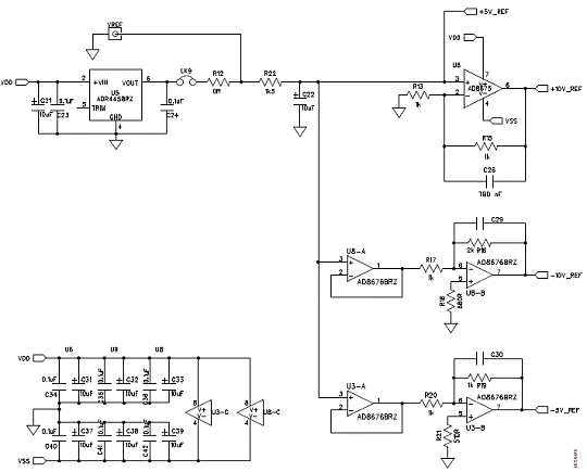
图5.评估板EVAL-AD5780电路图:电压参考电路
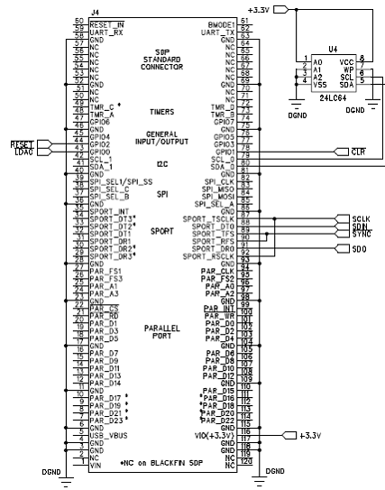
图6.评估板EVAL-AD5780电路图:SDP板连接器
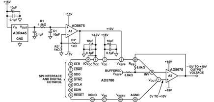
图7. 18位精度±10V电压源简化电路图
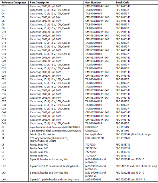
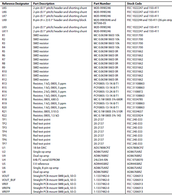
评估板EVAL-AD5780材料清单:
责任编辑:HanFeng
【免责声明】
1、本文内容、数据、图表等来源于网络引用或其他公开资料,版权归属原作者、原发表出处。若版权所有方对本文的引用持有异议,请联系拍明芯城(marketing@iczoom.com),本方将及时处理。
2、本文的引用仅供读者交流学习使用,不涉及商业目的。
3、本文内容仅代表作者观点,拍明芯城不对内容的准确性、可靠性或完整性提供明示或暗示的保证。读者阅读本文后做出的决定或行为,是基于自主意愿和独立判断做出的,请读者明确相关结果。
4、如需转载本方拥有版权的文章,请联系拍明芯城(marketing@iczoom.com)注明“转载原因”。未经允许私自转载拍明芯城将保留追究其法律责任的权利。
拍明芯城拥有对此声明的最终解释权。
相关资讯
:
基于MC33771主控芯片的新能源锂电池管理系统解决方案

AMIC110 32位Sitara ARM MCU开发方案

基于AMIC110多协议可编程工业通信处理器的32位Sitara ARM MCU开发方案

基于展讯SC9820超低成本LTE芯片平台的儿童智能手表解决方案

基于TI公司的AM437x双照相机参考设计

基于MTK6580芯片的W2智能手表解决方案


 2012- 2022 拍明芯城ICZOOM.com 版权所有 客服热线:400-693-8369 (9:00-18:00)


