


 产品分类
产品分类
ADI ADXL362微功耗三轴MEMS加速度计解决方案
 113
113
 拍明
拍明
原标题:ADI ADXL362微功耗三轴MEMS加速度计解决方案
ADI公司的ADXL362是微功耗三轴MEMS加速度计,数字输出,加速度范围为±2/±4/±8 g, 工作电压1.8V-3.3V,电源电压2V和100Hz输出数据速率时的功耗为2μA,运动触发叫醒模式的功耗为300nA,器件提供12位输出分辨率,8位格式的数据,在±2 g范围的分辨率为1 mg/LSB,主要用在助听器,家庭保健设备,运动使能电源开关,无线传感器和运动使能计量设备.本文介绍了ADXL362主要特性, ADXL362功能方框图以及评估板EVAL-ADXL362Z主要特性和电路图.
ADXL362: Micropower 3-Axis MEMS Accelerometer: Digital Output, ±2/±4/±8 g Range
The ADXL362 is an ultra-low power 3-axis MEMS accelerometer that consumes less than 2 μA at a 100 Hz output data rate, and 300 nA in motion-triggered Wake-Up Mode.
Unlike accelerometers that use power duty cycling to achieve low power consumption, the ADXL362 does not alias input signals by undersampling; it samples the sensor’s full bandwidth at all data rates.
The ADXL362 always provides 12-bit output resolution; 8-bit formatted data is also provided for more efficient single-byte transfers when a lower resolution is sufficient. Measurement ranges of ±2 g, ±4 g, and ±8 g are available, with a resolution of 1 mg/LSB on the ±2 g range. For applications where a noise level lower than the ADXL362’s normal 550 μg/7Hz is desired, either of two lower noise modes (down to 175 μg/7Hz typ) may be selected at minimal increase in supply current.
In addition to its ultra-low power consumption, the ADXL362 has many features to enable true system-level power reduction.
It includes a deep multimode output FIFO, a built-in micropower temperature sensor, and several activity detection modes including adjustable-threshold sleep and wakeup operation that can run as low as 300 nA at a 6 Hz (approximate) measurement rate. A pin output is provided to directly control an external switch when activity is detected if desired. In addition, the ADXL362 has provisions for external control of sampling time and/or an external clock.
The ADXL362 operates on a wide 1.6 V to 3.6 V supply range, and can interface, if necessary, to a host operating on a separate, lower supply voltage. The ADXL362 is available in a 3 mm × 3.25 mm × 1.06 mm package.
ADXL362主要特性:
Ultra low power
Power can be derived from coin cell battery
1.8 μA @ 100 Hz ODR, 2.0V supply
3.0 μA @ 400 Hz ODR, 2.0V supply
300 nA motion-activated Wake-up Mode
10nA Standby Current
Built-in features for system-level power savings:
Adjustable-threshold sleep/wake modes for motion activation
Autonomous interrupt processing without need for microcontroller intervention, so the rest of the system can be turned off completely
Deep embedded FIFO minimizes host processor load
Awake state output enables implementation of standalone motion-activated switch High resolution of 1 mg/LSB
Low noise down to 175 μg/@Hz
Wide supply and I/O voltage ranges: 1.6 V to 3.6 V
Operates off 1.8V to 3.3V rails
Acceleration sample synchronization via external trigger
On-chip temperature sensor
SPI digital interface
Measurement ranges selectable via SPI command
Small and thin 3 mm × 3.25 mm × 1.06 mm package
ADXL362应用:
Hearing aids
Home healthcare devices
Motion-enabled power save switch
Wireless sensors
Motion-enabled metering devices
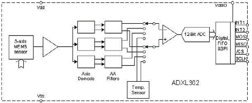
图1. ADXL362功能方框图
ADXL362评估板EVAL-ADXL362Z
The EVAL-ADXL362Z is a simple breakout board that enables easy connection of an ADXL362 micropower, 3-axis, digital-output MEMS accelerometer into an existing system. Due to its small size, the EVAL-ADXL362Z has minimal effect on performance of the system and of the accelerometer, and thus it is ideal for evaluation of the ADXL362 in an existing system. Note that the ADXL362 must be communicated with digitally via SPI. No processor is included with the EVAL-ADXL362Z; firmware must be supplied externally by the user. Some sample firmware is available at the link below:
The EVAL-ADXL362Z-MLP is a complete system for real-time evaluation of the ADXL362 micropower, 3-axis, digital-ouptut MEMS accelerometer. This system is accompanied by a graphical user interface (GUI) that facilitates evaluation of parameters such as power consumption, temperature coefficient, noise, and more. The system consists of a motherboard and a satellite board. The sensor is housed in a socket on the satellite board, enabling evaluation of multiple parts using one evaluation system.
To order the complete system, order the EVAL-ADXL362Z-MLP. This kit includes a motherboard, satellite board, accelerometer, and cables. Additional satellite board kits can be ordered using the part number EVAL-ADXL362Z-S. Satellite kit orders include a satellite board and an accelerometer.
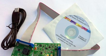
图2. 评估板EVAL-ADXL362Z外形图
责任编辑:HanFeng
【免责声明】
1、本文内容、数据、图表等来源于网络引用或其他公开资料,版权归属原作者、原发表出处。若版权所有方对本文的引用持有异议,请联系拍明芯城(marketing@iczoom.com),本方将及时处理。
2、本文的引用仅供读者交流学习使用,不涉及商业目的。
3、本文内容仅代表作者观点,拍明芯城不对内容的准确性、可靠性或完整性提供明示或暗示的保证。读者阅读本文后做出的决定或行为,是基于自主意愿和独立判断做出的,请读者明确相关结果。
4、如需转载本方拥有版权的文章,请联系拍明芯城(marketing@iczoom.com)注明“转载原因”。未经允许私自转载拍明芯城将保留追究其法律责任的权利。
拍明芯城拥有对此声明的最终解释权。
相关资讯
:
基于MC33771主控芯片的新能源锂电池管理系统解决方案

AMIC110 32位Sitara ARM MCU开发方案

基于AMIC110多协议可编程工业通信处理器的32位Sitara ARM MCU开发方案

基于展讯SC9820超低成本LTE芯片平台的儿童智能手表解决方案

基于TI公司的AM437x双照相机参考设计

基于MTK6580芯片的W2智能手表解决方案


 2012- 2022 拍明芯城ICZOOM.com 版权所有 客服热线:400-693-8369 (9:00-18:00)


