基于TI公司的TPS65580 4.5V至18V三通道同步降压转换器参考设计方案
 84
84
 拍明
拍明
原标题:TI TPS65580 4.5V至18V三通道同步降压转换器参考设计方案
TI公司的TPS65580是一款先进三端输出 D-CAP2™模式同步降压转换器芯片,该芯片使系统设计工程师在完成为多种终端设备提供电源稳压器时,提供具有成本效益、低器件数量、低待机电流的解决方案。TPS65580芯片主控回路采用D-CAP2™模式控制,使得在没有外部补偿器件的情况下,提供高效快速的瞬态响应。本文首先介绍芯片的简介、特性、内部框图及应用领域,并给出相应设计方案的设计原理图及元器件列表。
The TPS65580 is a triple, advanced D-CAP2™ mode synchronous buck converter. The TPS65580 enables system designers to complete the suite of various end equipment’s power bus regulators with a cost effective, low component count, and low standby current solution. The main control loops of the TPS65580 uses the advanced D-CAP2™ mode control which provides a fast transient response with no external compensation components. The TPS65580 is able to adapt to both low equivalent series resistance (ESR) output capacitors such as POSCAP or SP-CAP, and ultra-low ESR, ceramic capacitors. The device provides convenient and efficient operation with input voltages from 4.5V to 18V.
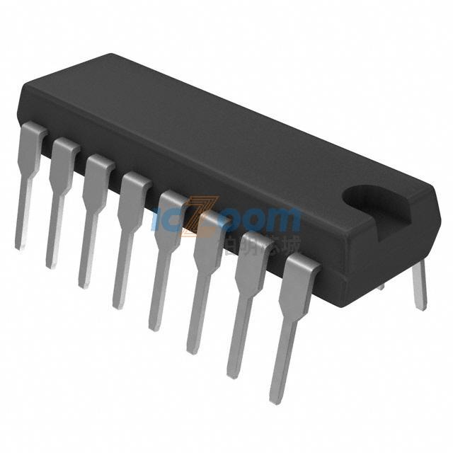
The TPS65580 is available in 4.4mm × 6.5mm 20 pin TSSOP (PWP) package, and is specified from –40°C to 85°C ambient temperature range.
TPS65580主要特性:
Advanced D-CAP2 Control Mode
Fast Transient Response
No External Parts Required For Loop Compensation
Compatible with Ceramic Output Capacitors
Wide Input Voltage Range : 4.5 V to 18 V
Output Voltage Range: 0.76 V to 7.0 V
Highly Efficient Integrated FETs Optimized for Low Duty Cycle Applications
160 mΩ (High Side) and 130 mΩ (Low Side) for 2.5A
250mΩ (High Side) and 230mΩ (Low Side) for 1.5A
High Initial Reference Accuracy
Low-Side RDS(on) Loss-Less Current Sensing
Fixed 1.2 ms Soft Start
Non-Sinking Pre-Biased Soft Start
700 kHz Switching frequency
Cycle-by-Cycle Over-Current Limiting Control
OCL, OVP, UVP, UVLO, TSD Protections
Hiccup Timer for Over Load Protection
PowerGood
Adaptive Gate Drivers with Integrated Boost PMOS Switch
OCP Constant Due To Thermally Compensated rds(on) with 4000ppm/°
20-Pin HTSSOP
TPS65580应用:
Point-of-Load Regulation in Low Power Systems for Wide Range of Applications
Digital TV Power Supply
Networking Home Terminal
Digital Set Top Box (STB)
DVD Player/Recorder
Gaming Consoles and Other

图1. TPS65580内部方框图
TPS65580方案介绍:
The Texas Instruments TPS65580EVM-575 evaluation module (EVM) is a fully assembled and tested circuit for evaluating the TPS65580 Synchronous Step-Down Converter. The EVM comprises a nominal 12 V input output synchronous buck converter with three output channels. Output channel 1 is 3.3 V at 1.5 A, channel 2 is 1.2 V at 2.0 A, and channel 3 is 1.5 V at 1.5 A. The input voltage range is 4.5 V to 18 V. The TPS65580 features enable control for each output channel and a combined power good function. The TPS65580 uses DCAP2 control with pseudo fixed 700 kHz switching frequency for fast transient response with minimal output capacitance.
Features
Synchronous Buck Converter
3 CH output
Internal Slow Start
Wide Input Voltage up to 18 V
Integrated FETs
TPS65580方案材料清单:

PCB元件布局图:

责任编辑:HanFeng
【免责声明】
1、本文内容、数据、图表等来源于网络引用或其他公开资料,版权归属原作者、原发表出处。若版权所有方对本文的引用持有异议,请联系拍明芯城(marketing@iczoom.com),本方将及时处理。
2、本文的引用仅供读者交流学习使用,不涉及商业目的。
3、本文内容仅代表作者观点,拍明芯城不对内容的准确性、可靠性或完整性提供明示或暗示的保证。读者阅读本文后做出的决定或行为,是基于自主意愿和独立判断做出的,请读者明确相关结果。
4、如需转载本方拥有版权的文章,请联系拍明芯城(marketing@iczoom.com)注明“转载原因”。未经允许私自转载拍明芯城将保留追究其法律责任的权利。
拍明芯城拥有对此声明的最终解释权。


 产品分类
产品分类




 2012- 2022 拍明芯城ICZOOM.com 版权所有 客服热线:400-693-8369 (9:00-18:00)


