


 产品分类
产品分类
基于TI公司的CC2541蓝牙邮票块参考设计
 181
181
 拍明
拍明
原标题:TI CC2541蓝牙邮票块参考设计
TI公司的CC2541是用于蓝牙低功耗和2.4GHz应用的真正系统级芯片(SoC),器件集成了RF和高性能低功耗8051 MCU内核,支持250kbps, 500kbps, 1Mbps和2Mbps数据速率,可编输出功率高达0dBm,1Mbps时的接收灵敏度–94 dBm,主要用在2.4GHz蓝牙低功耗系统,人机接口如键盘,鼠标和遥控,体验生活和休闲设备,手机和消费类电子.本文介绍了CC2541主要特性,框图和典型应用电路,以及邮票大小的蓝牙模块的参考设计主要特性,电路图,材料清单和PCB元件布局图.
The CC2541 is a power-optimized true system-on-chip (SoC) solution for both Bluetooth low energy and proprietary 2.4-GHz applications. It enables robust network nodes to be built with low total bill-of-material costs. The CC2541 combines the excellent performance of a leading RF transceiver with an industry-standard enhanced 8051 MCU, in-system programmable flash memory, 8-KB RAM, and many other powerful supporting features and peripherals. The CC2541 is highly suited for systems where ultralow power consumption is required. This is specified by various operating modes. Short transition times between operating modes further enable low power consumption.
The CC2541 is pin-compatible with the CC2540 in the 6-mm × 6-mm QFN40 package, if the USB is not used on the CC2540 and the I2C/extra I/O is not used on the CC2541. Compared to the CC2540, the CC2541 provides lower RF current consumption. The CC2541 does not have the USB interface of the CC2540, and provides lower maximum output power in TX mode. The CC2541 also adds a HW I2C interface.
The CC2541 is pin-compatible with the CC2533 RF4CE-optimized IEEE 802.15.4 SoC.
The CC2541 comes in two different versions: CC2541F128/F256, with 128 KB and 256 KB of flash memory, respectively.
CC2541主要特性:
RF
2.4-GHz Bluetooth low energy Compliant and Proprietary RF System-on-Chip
Supports 250-kbps, 500-kbps, 1-Mbps, 2-Mbps Data Rates
Excellent Link Budget, Enabling Long-Range Applications Without External Front End
Programmable Output Power up to 0 dBm
Excellent Receiver Sensitivity (–94 dBm at 1 Mbps), Selectivity,
and Blocking Performance
Suitable for Systems Targeting Compliance With Worldwide Radio
Frequency Regulations: ETSI EN 300 328 and EN 300 440 Class 2 (Europe),
FCC CFR47 Part 15 (US), and ARIB STD-T66 (Japan)
Layout
Few External Components
Reference Design Provided
6-mm × 6-mm QFN-40 Package
Pin-Compatible With CC2540 (When Not Using USB or I2C)
Low Power
Active-Mode RX Down to: 17.9 mA
Active-Mode TX (0 dBm): 18.2 mA
Power Mode 1 (4-µs Wake-Up): 270 µA
Power Mode 2 (Sleep Timer On): 1 µA
Power Mode 3 (External Interrupts): 0.5 µA
Wide Supply-Voltage Range (2 V–3.6 V)
TPS62730 Compatible Low Power in Active Mode
RX Down to: 14.7 mA (3-V supply)
TX (0 dBm): 14.3 mA (3-V supply)
Microcontroller
High-Performance and Low-Power 8051 Microcontroller Core With Code Prefetch
In-System-Programmable Flash, 128- or 256-KB
8-KB RAM With Retention in All Power Modes
Hardware Debug Support
Extensive Baseband Automation, Including Auto-Acknowledgment and Address Decoding
Retention of All Relevant Registers in All Power Modes
Peripherals
Powerful Five-Channel DMA
General-Purpose Timers (One 16-Bit, Two 8-Bit)
IR Generation Circuitry
32-kHz Sleep Timer With Capture
Accurate Digital RSSI Support
Battery Monitor and Temperature Sensor
12-Bit ADC With Eight Channels and Configurable Resolution
AES Security Coprocessor
Two Powerful USARTs With Support for Several Serial protocols
23 General-Purpose I/O Pins (21 × 4 mA, 2 × 20 mA)
I2C interface
2 I/O Pins Have LED Driving Capabilities
Watchdog Timer
Integrated High-PerformanceComparator
Development Tools
CC2541 Evaluation Module Kit (CC2541EMK)
CC2541 Mini Development Kit (CC2541DK-MINI)
SmartRF™ Software
IAR Embedded Workbench™ Available
软件特性:
Bluetooth v4.0 Compliant Protocol Stack for Single-Mode BLE Solution
Complete Power-Optimized Stack, Including Controller and HostGAP – Central, Peripheral, Observer, or Broadcaster (Including Combination Roles)ATT / GATT – Client and ServerSMP – AES-128 Encryption and DecryptionL2CAP
Sample Applications and Profiles
Generic Applications for GAP Central and Peripheral Roles
Proximity, Accelerometer, Simple Keys, and Battery GATT Services
More Applications Supported in BLE Software Stack
Multiple Configuration Options
Single-Chip Configuration, Allowing Applications to Run on CC2541
Network Processor Interface for Applications Running on an External Microcontroller
BTool – Windows PC Application for Evaluation, Development, and Test
CC2541主要应用:
• 2.4-GHz Bluetooth low energy Systems
• Proprietary 2.4-GHz Systems
• Human-Interface Devices (Keyboard, Mouse,Remote Control)
• Sports and Leisure Equipment
• Mobile Phone Accessories
• Consumer Electronics
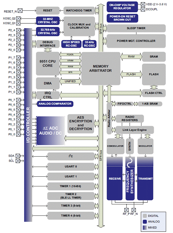
图1. CC2541框图

图2. CC2541应用电路
CC2541蓝牙邮票块参考设计
The CC2541 Postage Stamp reference design contains the schematics and layout files for the CC2541PS Module. The reference design demonstrates good techniques for CC2541 decoupling and RF layout for a very compact 16.3mm x 13mm PCB . For optimum RF performance, the reference design should be copied accurately. This is a 2-layer PCB reference design using an integrated solution of a Johanson Chip balun(2450BM15A0002) and a Johanson chip antenna(2450AT42A100). The CC2541 Postage stamp is perfect for applications requiring proximity detecting and temperature sensing. It is ideal for proof of concept prototyping on existing systems.
CC2541蓝牙邮票块参考设计主要特性:
Affordable low cost, 2 layer board design in a compact form factor of 16.3mmX13mm
Onboard chip antenna (from Johanson, 2450AT42A100) with integrated balun (from Johanson, 2450BM15A002) matching circuit, with 1 SPI, 1 I2C and 1 USART interface pinout
Can be used for proximity sensing, temp data logging, quick prototyping and quick PoC (Proof of Concept) purposes
Free schematics, BOM and gerber available online for download
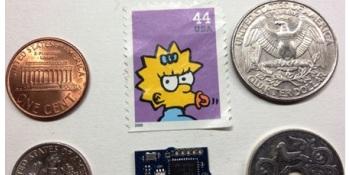
图3.CC2541蓝牙邮票块参考设计外形图
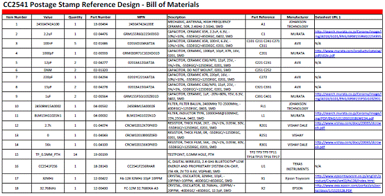
CC2541蓝牙邮票块参考设计材料清单:
责任编辑:HanFeng
【免责声明】
1、本文内容、数据、图表等来源于网络引用或其他公开资料,版权归属原作者、原发表出处。若版权所有方对本文的引用持有异议,请联系拍明芯城(marketing@iczoom.com),本方将及时处理。
2、本文的引用仅供读者交流学习使用,不涉及商业目的。
3、本文内容仅代表作者观点,拍明芯城不对内容的准确性、可靠性或完整性提供明示或暗示的保证。读者阅读本文后做出的决定或行为,是基于自主意愿和独立判断做出的,请读者明确相关结果。
4、如需转载本方拥有版权的文章,请联系拍明芯城(marketing@iczoom.com)注明“转载原因”。未经允许私自转载拍明芯城将保留追究其法律责任的权利。
拍明芯城拥有对此声明的最终解释权。
相关资讯
:
基于MC33771主控芯片的新能源锂电池管理系统解决方案

AMIC110 32位Sitara ARM MCU开发方案

基于AMIC110多协议可编程工业通信处理器的32位Sitara ARM MCU开发方案

基于展讯SC9820超低成本LTE芯片平台的儿童智能手表解决方案

基于TI公司的AM437x双照相机参考设计

基于MTK6580芯片的W2智能手表解决方案


 2012- 2022 拍明芯城ICZOOM.com 版权所有 客服热线:400-693-8369 (9:00-18:00)


