


 产品分类
产品分类
基于NXP公司的LPC81xM 32位ARM Cortex-M0+ MCU开发方案
 100
100
 拍明
拍明
原标题:NXP LPC81xM 32位ARM Cortex-M0+ MCU开发方案
nxp公司的LPC81xM系列产品是基于ARM Cortex-M0+内核的低成本32位MCU,CPU工作频率高达30MHz,支持高达16KB闪存和4KB SRAM,外设包括CRC引擎,I2C总线接口,多达三个UART,多达两个SPI接口,一个多速率定时器,自叫醒定时器和状态可配置的定时器,一个比较器,功能可配置的I/O端口和多达18个通用I/O引脚,主要用于照明, 消费类电子,马达控制,火警和安防和气候控制.本文介绍了LPCXpresso812 MAX主要特性和优势,框图, 评估板LPCXpresso812-MAX主要特性和电路图.
The LPC81xM are an ARM Cortex-M0+ based, low-cost 32-bit MCU family operating at CPU frequencies of up to 30 MHz. The LPC81xM support up to 16 kB of flash memory and 4 kB of SRAM.
The peripheral complement of the LPC81xM includes a CRC engine, one I2C-bus interface, up to three USARTs, up to two SPI interfaces, one multi-rate timer, self wake-up timer, and state-configurable timer, one comparator, function-configurable I/O ports through a switch matrix, an input pattern match engine, and up to 18 general-purpose I/O pins.
LPCXpresso812 MAX主要特性和优势:
System:
ARM Cortex-M0+ processor, running at frequencies of up to 30 MHz with single-cycle multiplier and fast single-cycle I/O port.
ARM Cortex-M0+ built-in Nested Vectored Interrupt Controller (NVIC).
System tick timer.
Serial Wire Debug (SWD) and JTAG boundary scan modes supported.
Micro Trace Buffer (MTB) supported.
Memory:
Up to 16 kB on-chip flash programming memory with 64 Byte page write and erase.
Up to 4 kB SRAM.
ROM API support:
Boot loader.
USART drivers.
I2C drivers.
Power profiles.
Flash In-Application Programming (IAP) and In-System Programming (ISP).
Digital peripherals:
High-speed GPIO interface connected to the ARM Cortex-M0+ IO bus with up to 18 General-Purpose I/O (GPIO) pins with configurable pull-up/pull-down resistors, programmable open-drain mode, input inverter, and glitch filter.
High-current source output driver (20 mA) on four pins.
High-current sink driver (20 mA) on two true open-drain pins.
GPIO interrupt generation capability with boolean pattern-matching feature on eight GPIO inputs.
Switch matrix for flexible configuration of each I/O pin function.
State Configurable Timer/PWM (SCTimer/PWM) with input and output functions (including capture and match) assigned to pins through the switch matrix.
Multiple-channel multi-rate timer (MRT) for repetitive interrupt generation at up to four programmable, fixed rates.
Self Wake-up Timer (WKT) clocked from either the IRC or a low-power, low-frequency internal oscillator.
CRC engine.
Windowed Watchdog timer (WWDT).
Analog peripherals:
Comparator with internal and external voltage references with pin functions assigned or enabled through the switch matrix.
Serial interfaces:
Three USART interfaces with pin functions assigned through the switch matrix.
Two SPI controllers with pin functions assigned through the switch matrix.
One I2C-bus interface with pin functions assigned through the switch matrix.
Clock generation:
12 MHz internal RC oscillator trimmed to 1.5 % accuracy that can optionally be used as a system clock.
Crystal oscillator with an operating range of 1 MHz to 25 MHz.
Programmable watchdog oscillator with a frequency range of 9.4 kHz to 2.3 MHz.
10 kHz low-power oscillator for the WKT.
PLL allows CPU operation up to the maximum CPU rate without the need for a high-frequency crystal. May be run from the system oscillator, the external clock input CLKIN, or the internal RC oscillator.
Clock output function with divider that can reflect the crystal oscillator, the main clock, the IRC, or the watchdog oscillator.
Power control:
Integrated PMU (Power Management Unit) to minimize power consumption.
Reduced power modes: Sleep mode, Deep-sleep mode, Power-down mode, and Deep power-down mode.
Wake-up from Deep-sleep and Power-down modes on activity on USART, SPI, and I2C peripherals.
Timer-controlled self wake-up from Deep power-down mode.
Power-On Reset (POR).
Brownout detect.
Unique device serial number for identification.
Single power supply.
Operating temperature range -40 ℃ to 105 ℃ except for the DIP8 package, which is available for a temperature range of -40 ℃ to 85 ℃.
Available as DIP8, TSSOP16, SO20, TSSOP20, and XSON16 package
LPCXpresso812 MAX应用:
8/16-bit applications
Lighting
Consumer
Motor control
Climate control
Fire and security applications
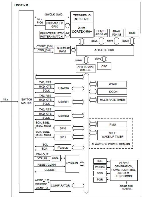
图1. LPCXpresso812 MAX框图
评估板LPCXpresso812-MAX
The LPCXpresso812-MAX board with NXP’s LPC812 Cortex-M0+ microcontroller is designed to make it as easy as possible to get started with your project.
LPCXpresso™ is a low-cost development platform available from NXP, supporting NXP’s ARM-based microcontrollers. The platform is comprised of a simplified Eclipse-based IDE and low-cost target boards which include an attached JTAG debugger. LPCXpresso is an end-to-end solution enabling embedded engineers to develop their applications from initial evaluation to final production.
评估板LPCXpresso812-MAX主要特性:
Fully supported by LPCXpresso Eclipse-based IDE and GNU C/C++ toolchain, available in free and Pro versions
Works with by Keil, IAR and other toolchains with CMSIS-DAP support
Integrated JTAG Debugger which can also be used to debug external target
LPCXpresso / mbed and Arduino UNO expansion connectors give simple access to a wide range of available expansion boards
Embedded Artists 14-pin expansion connector
Tri-color LED
On-board ADC
Reset and User interrupt buttons for easy testing of software functionality
The LPCXpresso-MAX family of boards provide a powerful and flexible development system for some of NXP’s low end MCUs. They can be used out of the box with a range of development tools, including the LPCXpresso IDE, as well as with ARM’s mbed online toolchain.
The standard LPCXpresso-MAX board design offers the following features:
Built in CMSIS-DAP based debug probe, based on the NXP LPC11U3x MCU.
Compatible with LPCXpresso IDE, mbed and other toolchains
Debug connector to allow debug of target MCU via an external probe.
Tri-color LED
Target ISP and WAKE buttons (LPCXpresso824-MAX)/User interrupt button
(LPCXpresso812-MAX)
Target Reset button
Expansion options:
MCU pins available on ‘standard LPCXpresso/mbed’ expansion connector (board bottom side)
Arduino connectors compatible with the ”Arduino UNO” platform (board top side)
Other expansion options (see board specific information below)
Powered from multiple sources
Link2 (debug probe) USB
LPCXpresso/mbed header
Options to allow measurement of current consumed by target MCU
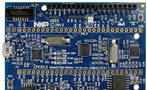
图2. 评估板LPCXpresso812-MAX外形图
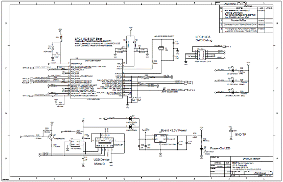
图3. 评估板LPCXpresso812-MAX电路图(1)
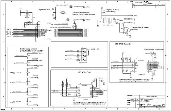
图4. 评估板LPCXpresso812-MAX电路图(2)
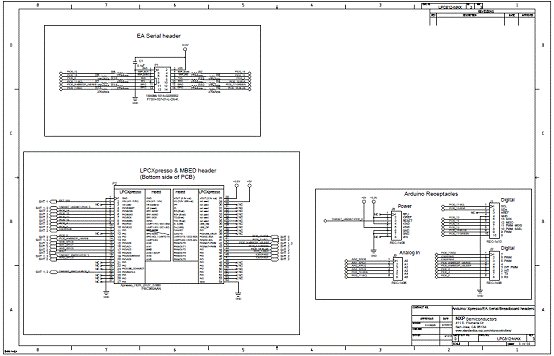
图5. 评估板LPCXpresso812-MAX电路图(3)
责任编辑:HanFeng
【免责声明】
1、本文内容、数据、图表等来源于网络引用或其他公开资料,版权归属原作者、原发表出处。若版权所有方对本文的引用持有异议,请联系拍明芯城(marketing@iczoom.com),本方将及时处理。
2、本文的引用仅供读者交流学习使用,不涉及商业目的。
3、本文内容仅代表作者观点,拍明芯城不对内容的准确性、可靠性或完整性提供明示或暗示的保证。读者阅读本文后做出的决定或行为,是基于自主意愿和独立判断做出的,请读者明确相关结果。
4、如需转载本方拥有版权的文章,请联系拍明芯城(marketing@iczoom.com)注明“转载原因”。未经允许私自转载拍明芯城将保留追究其法律责任的权利。
拍明芯城拥有对此声明的最终解释权。
相关资讯
:
基于MC33771主控芯片的新能源锂电池管理系统解决方案

AMIC110 32位Sitara ARM MCU开发方案

基于AMIC110多协议可编程工业通信处理器的32位Sitara ARM MCU开发方案

基于展讯SC9820超低成本LTE芯片平台的儿童智能手表解决方案

基于TI公司的AM437x双照相机参考设计

基于MTK6580芯片的W2智能手表解决方案


 2012- 2022 拍明芯城ICZOOM.com 版权所有 客服热线:400-693-8369 (9:00-18:00)


