


 产品分类
产品分类
基于ST公司的STGAP1S gapDRIVE电隔离N-MOSFET栅极驱动解决方案
 119
119
 拍明
拍明
原标题:ST STGAP1S gapDRIVE电隔离N-MOSFET栅极驱动解决方案
ST公司的STGAP1S gapDRIVE是电隔离N-MOSFET栅极驱动器,具有先进的保护,配置和诊断特性.驱动器驱动能力为5A,高压部分高达1500V,输入-输出延迟100ns,提供很高的PWM控制精度,主要用在600/1200V逆变器,工业驱动,DC/DC转换器,UPS设备和太阳能逆变器.本文介绍了STGAP1S gapDRIVE主要特性,框图,半桥配置应用框图以及评估板EVALSTGAP1S主要特性, 单驱动配置图,半桥驱动配置图,电路图和材料清单.
The STGAP1S gapDRIVE™ is a galvanically isolated single gate driver for N-channel MOSFETs and IGBTs with advanced protection, configuration and diagnostic features. The architecture of the STGAP1S isolates the channel from the control and the low voltage interface circuitry through true galvanic isolation.
The gate driver is characterized by 5 A capability, making the device also suitable for high power inverter applications such as motor drivers in industrial drives. The output driver section provides a rail-to-rail output with the possibility to use a negative gate driver supply.
The input to output propagation delay results contained within 100 ns, providing high PWM control accuracy. Protection functions such as the Miller clamp, desaturation detection, dedicated sense pin for overcurrent detection, output 2-level turn-off, VCE overvoltage protection, UVLO and OVLO are included to easily design high reliability systems.Open drain diagnostic outputs are present and detailed device conditions can be monitored through the SPI. Each function’s parameter can be programmed via the SPI, making the device very flexible and allowing it to fit in a wide range of applications.Separate sink and source outputs provide high flexibility and bill of material reduction for external components.
STGAP1S gapDRIVE主要特性:
High voltage rail up to 1500 V
Driver current capability: 5 A sink/source current at 25 ℃
dV/dt transient immunity ± 50 V/ns in full temperature range
Overall input/output propagation delay: 100 ns
Separate sink and source for easy gate driving configuration
Negative gate drive ability
Active Miller clamp
Desaturation detection
SENSE input
VCE active clamping
Output 2-level turn-off
Diagnostic status output
UVLO and OVLO functions
Programmable input deglitch filter
Asynchronous stop command
Programmable deadtime, with violation error
SPI interface for parameters programming
Temperature warning and shutdown protection
Self-diagnostic routines for protection features
Compact and simplified layout
Full effective fault protection
STGAP1S gapDRIVE应用:
600/1200 V inverters
Industrial drives
UPS equipment
DC/DC converters
Solar inverters
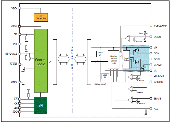
图1. STGAP1S gapDRIVE框图
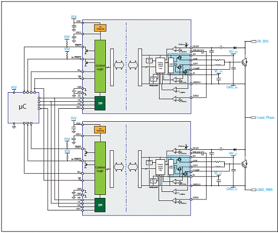
图2. STGAP1S gapDRIVE半桥配置应用框图
评估板EVALSTGAP1S
Demonstration board for gapDRIVE: galvanically isolated single high voltage gate driver The STGAP1S gapDRIVE™ is a galvanically isolated single gate driver for N-channel MOSFETs and IGBTs with advanced protection,configuration and diagnostic features. The architecture of the STGAP1S isolates the channel from the control and the low voltage interface circuitry through true galvanic isolation.
The EVALSTGAP1S board allows evaluating all of the STGAP1S features while driving a power switch with a voltage rating up to 1500 V. Power switches in both TO-220 or TO-247 packages can be evaluated, and the board allows the connection of a heatsink in order to exploit the ability of the STGAP1S to handle very high power applications.
In combination with the STEVAL-PCC009V2 communication board and the gapDRIVE™ evaluation software, the board allows to easily enable, configure or disable all of the driver’s protection and control features through the SPI interface. Advanced diagnostic is also available thanks to the driver’s status registers that can be accessed through the SPI.
Multiple boards can be connected together and share the same logic supply voltage and control signals in order to evaluate half-bridge, interleaved or even more complex topologies. The board allows implementing the SPI daisy chain when more than one device is used.
评估板EVALSTGAP1S 主要特性:
High voltage rail up to 1500 V
5 A sink/source driver current capability
5 A active Miller clamp
Gate driving voltage up to 36 V
Negative gate driving ability
Desaturation detection
Overcurrent protection
Output 2-level turn-off (2LTO) UVLO on each supply voltage
Overtemperature warning and shut-down protection
3.3/5 V logic input interface
Optimized reference layout
SPI with daisy chain feature for parameters programming and diagnostic
Suitable to be used in combination with STEVAL-PCC009V2 and configuration GUI
Fault LED indicators
RoHS compliant
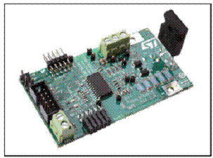
图3.评估板EVALSTGAP1S外形图
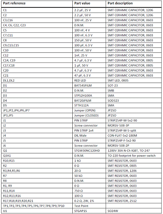
评估板EVALSTGAP1S材料清单:
责任编辑:HanFeng
【免责声明】
1、本文内容、数据、图表等来源于网络引用或其他公开资料,版权归属原作者、原发表出处。若版权所有方对本文的引用持有异议,请联系拍明芯城(marketing@iczoom.com),本方将及时处理。
2、本文的引用仅供读者交流学习使用,不涉及商业目的。
3、本文内容仅代表作者观点,拍明芯城不对内容的准确性、可靠性或完整性提供明示或暗示的保证。读者阅读本文后做出的决定或行为,是基于自主意愿和独立判断做出的,请读者明确相关结果。
4、如需转载本方拥有版权的文章,请联系拍明芯城(marketing@iczoom.com)注明“转载原因”。未经允许私自转载拍明芯城将保留追究其法律责任的权利。
拍明芯城拥有对此声明的最终解释权。
相关资讯
:
基于MC33771主控芯片的新能源锂电池管理系统解决方案

AMIC110 32位Sitara ARM MCU开发方案

基于AMIC110多协议可编程工业通信处理器的32位Sitara ARM MCU开发方案

基于展讯SC9820超低成本LTE芯片平台的儿童智能手表解决方案

基于TI公司的AM437x双照相机参考设计

基于MTK6580芯片的W2智能手表解决方案


 2012- 2022 拍明芯城ICZOOM.com 版权所有 客服热线:400-693-8369 (9:00-18:00)


