基于Lattice公司的MachXO3L低成本高密度I-O扩展解决方案
 77
77
 拍明
拍明
原标题:Lattice MachXO3L低成本高密度I-O扩展解决方案
lattice公司的MachXO3L是低成本高密度I-O扩展器,有C版本和E版本两种器件, C版本工作电压3.3V或2.5V, E版本工作电压1.2V,封装尺寸从2.5 x 2.5 mm WLCSP 到17 x 17 mm caBGA,多达335个I/O引脚,主要用在消费类电子,计算与存储,无线通信,工业控制和汽车电子.本文介绍了MachXO3L系列主要特性, MachXO器件框图和MachXO3L-4300器件框图,以及MachXO3L分接板评估套件主要特性,框图和电路图.
The MachXO3L devices are available in two versions C and E with two speed grades: -5 and -6, with -6 being the fastest. C devices have an internal linear voltage regulator which supports external VCC supply voltages of 3.3 V or 2.5 V. E devices only accept 1.2 V as the external VCC supply voltage. With the exception of power supply voltage both C and E are functionally compatible with each other. The MachXO3L PLDs are available in a broad range of advanced halogen-free packages ranging from the space saving 2.5 x 2.5 mm WLCSP to the 17 x 17 mm caBGA. MachXO3L devices support density migration within the same package. Table 1-1 shows the LUT densities, package and I/O options, along with other key parameters. The MachXO3L devices offer enhanced I/O features such as drive strength control, slew rate control, PCI compatibility, bus-keeper latches, pull-up resistors, pull-down resistors, open drain outputs and hot socketing. Pull-up, pull-down and bus-keeper features are controllable on a “per-pin” basis. A user-programmable internal oscillator is included in MachXO3L devices. The clock output from this oscillator may be divided by the timer/counter for use as clock input in functions such as LED control, key-board scanner and similar state machines.
The MachXO3L devices also provide flexible, reliable and secure configuration from on-chip NVCM. These devices can also configure themselves from external SPI Flash or be configured by an external master through the JTAG test access port or through the I2C port. Additionally, MachXO3L devices support dual-boot capability (using exter-nal Flash memory) and remote field upgrade (TransFR) capability. Lattice provides a variety of design tools that allow complex designs to be efficiently implemented using the MachXO3L family of devices. Popular logic synthesis tools provide synthesis library support for MachXO3L. Lattice design tools use the synthesis tool output along with the user-specified preferences and constraints to place and route the design in the MachXO3L device. These tools extract the timing from the routing and back-annotate it into the design for timing verification. Lattice provides many pre-engineered IP (Intellectual Property) LatticeCORE™ modules, including a number of reference designs licensed free of charge, optimized for the MachXO3L PLD family. By using these configurable soft core IP cores as standardized blocks, users are free to concentrate on the unique aspects of their design, increasing their productivity.
MachXO3L系列主要特性:
•High IO/logic, lowest cost/IO, high IO devices for IO expansion applications
•High IO to LUT ratio with up to 335 IO pins
•0.8mm pitch: 1K to 6.9K densities with up to 335 IOs in BGA packages
•Generic DDR, DDRx2, DDRx4
- LVCMOS 3.3/2.5/1.8/1.5/1.2
- LVTTL
- LVDS, Bus-LVDS, MLVDS, LVPECL
- MIPI D-PHY Emulated
- Schmitt trigger inputs, up to 0.5 V hysteresis
- Wide input frequency range (7 MHz to 400 MHz)
- Powers up in microseconds
•Optional dual boot with external SPI memory
•In-field logic update while IO holds the system state
Solutions
• Smallest footprint, lowest power, high data throughput bridging solutions for mobile applica-tions
• Optimized footprint, logic density, IO count, IO performance devices for IO management and logic applications
Flexible Architecture
• Logic Density ranging from 640 to 6.9K LUT4
Advanced Packaging
• 0.4 mm pitch: 1K to 4K densities in very small footprint WLCSP (2.5 mm x 2.5 mm to 3.8 mm x 3.8 mm) with 28 to 63 IOs
• 0.5 mm pitch: 640 to 6.9K LUT densities in 6 mm x 6 mm to 10 mm x 10 mm BGA packages with up to 281 IOs
Pre-Engineered Source Synchronous I/O
• DDR registers in I/O cells
• Dedicated gearing logic
• 7:1 Gearing for Display I/Os
High Performance, Flexible I/O Buffer
• Programmable sysIOTM buffer supports wide range of interfaces:
• Ideal for IO bridging applications
• I/Os support hot socketing
• On-chip differential termination
• Programmable pull-up or pull-down mode
Flexible On-Chip Clocking
• Eight primary clocks
• Up to two edge clocks for high-speed I/O inter-faces (top and bottom sides only)
• Up to two analog PLLs per device with frac-tional-n frequency synthesis Non-volatile, Multi-time Programmable
• Instant-on
• Single-chip, secure solution
• Programmable through JTAG, SPI or I2C
TransFR Reconfiguration
Enhanced System Level Support
• On-chip hardened functions: SPI, I2C, timer/ counter
• On-chip oscillator with 5.5% accuracy
• Unique TraceID for system tracking
• Single power supply with extended operating range
• IEEE Standard 1149.1 boundary scan
• IEEE 1532 compliant in-system programming
MachXO3L 应用:
• Consumer Electronics
• Compute and Storage
• Wireless Communications
• Industrial Control Systems
• Automotive System

图1. MachXO器件框图(顶视图)

图2. MachXO3L-4300器件框图(顶视图)
MachXO3L分接板评估套件
The MachXO3L Breakout Board Evaluation Kit focuses on providing an environment to evaluate high speed source synchronous interfaces with the Lattice MachXO3L-2100 and MachXO3L-6900 products in both 49-ball WLCSP and 256-ball caBGA packages respectively. The MachXO3L Breakout Board contains two sections for development. The first section of the board features the MachXO3L-2100 which is optimized for MIPI D-PHY receiver and MIPI D-PHY transmitter interfaces with up to four data lanes and one clock lane each. The second section of the board features the MachXO3L-6900. This section provides a flexible IO evaluation environment for MIPI D-PHY, SubLVDS, FPD-LINK, FPC-LINK as well as other source synchronous type protocols. The IO of the MachXO3L-6900 provides eight high speed data and two high speed clock interfaces in both transmit and receive directions. Connection to these interfaces is available through SMAs for signal integrity and performance evaluation.
The MachXO3L Breakout Board allows for multi-device testing and scalability by providing a larger MachXO3L- 6900 and a smaller MachXO3L-2100 device. The MachXO3L-6900 has two high speed clock and eight high speed data inputs and outputs. By default these ports are configured for MIPI D-PHY IO support, but can be modified for various IO options, such as LVDS, SubLVDS and CMOS. The MachXO3L-6900 also has four general purpose IO headers, two of which have the ability to connect with Digilent PMOD interface boards. Additionally, the MachXO3L-6900 device has the ability to control four general purpose LEDs and one tri-color RGB LED. The MachXO3L-2100 is attached to two connectors providing four data and one clock lanes configured for MIPI D-PHY going in to and out of the FPGA. The pinout for the MachXO3L-2100 is optimized for low cost and small form factor by operating only off of 1.2 V and 3.3 V CMOS IO rails.
MachXO3L分接板主要特性:
Contains both the Lattice XO3L-2100 device in 49-ball WLCSP and the Lattice XO3L-6900 device in 256-ball caBGA package
The XO3L-2100 section is optimized for MIPI D-PHY receiver and transmitter interfaces
The XO3L-6900 section provides a flexible I/O evaluation environment for SubLVDS, FPD-LINK, FPC-LINK, MIPI D-PHY as well as other source-synchronous type protocols
Available with DSI connectors (LCMXO3L-DSI-EVN) or SMA (LCMXO3L-SMA-EVN) connectors
Evaluate CMOS I/Os, MIPI DSI, CSI-2 Tx and Rx capability, LED driving capability, programming via JTAG or I2C, SPI flash operation
MachXO3L分接板评估套件包括:
• MachXO3L Breakout Board
• Pre-loaded Demo
• Mini USB Cable
• QuickStart Guide

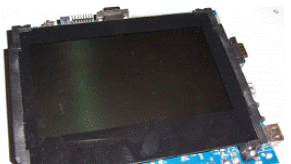
图3. MachXO3L分接板外形
责任编辑:HanFeng
【免责声明】
1、本文内容、数据、图表等来源于网络引用或其他公开资料,版权归属原作者、原发表出处。若版权所有方对本文的引用持有异议,请联系拍明芯城(marketing@iczoom.com),本方将及时处理。
2、本文的引用仅供读者交流学习使用,不涉及商业目的。
3、本文内容仅代表作者观点,拍明芯城不对内容的准确性、可靠性或完整性提供明示或暗示的保证。读者阅读本文后做出的决定或行为,是基于自主意愿和独立判断做出的,请读者明确相关结果。
4、如需转载本方拥有版权的文章,请联系拍明芯城(marketing@iczoom.com)注明“转载原因”。未经允许私自转载拍明芯城将保留追究其法律责任的权利。
拍明芯城拥有对此声明的最终解释权。


 产品分类
产品分类




 2012- 2022 拍明芯城ICZOOM.com 版权所有 客服热线:400-693-8369 (9:00-18:00)


