


 产品分类
产品分类
基于Freescale公司的Kinetis KE06 MCU开发方案
 103
103
 拍明
拍明
原标题:Freescale Kinetis KE06 MCU开发方案
freescale公司的Kinetis KE06 MCU采用ARM® Cortex®-M0+内核,工作频率48MHz,具有ESD/EMC性能和CAN,以及模拟,通信,定时和控制外设,以及不同容量的闪存(高达128KB)和引脚数.工作电压2.7V-5.5V,闪存写电压2.7V-5.5V,单周期32位x32位乘法器,主要用在家用电器,模拟电源,DC/DC转换器,DC风扇, 离线UPS,仪器仪表/PLC以及工业控制等.本文介绍了Kinetis KE06系列主要特性,框图, 开发平台FRDM-KE06Z主要特性,框图,电路图和材料清单.
The Kinetis KE0x family is the entry point into the Kinetis E series and is pin-compatible across the E series and with the 8-bit S08P family.
This family includes a powerful array of analog, communication, timing and control peripherals with varying flash memory size and pin count.Additionally, the series offers highly robust, cost-effective and energy-efficient MCUs that provide the appropriate entry-level solution. Ultimately, this product group is the next-generation MCU solution, offering enhanced ESD/ EMC performance for cost-sensitive, high-reliability device applications used in high electrical noise environments.
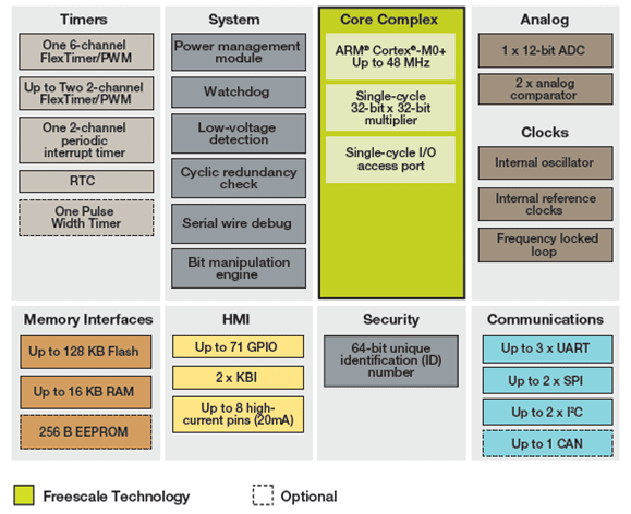
图1. Kinetis KE06系列MCU框图
Kinetis KE06系列主要特性:
Operating Characteristics
• Voltage range: 2.7 to 5.5 V
• Flash write voltage range: 2.7 to 5.5 V
• Temperature range (ambient): –40 ℃ to +105 ℃
Performance
• Up to 48 MHz ARM® Cortex®-M0+ core
• Single-cycle 32-bit x 32-bit multiplier
• Single-cycle I/O access port
Memories and Memory Interfaces
• Up to 128 KB flash
• Up to 16 KB RAM
• Up to 256 B EEPROM
Clocks
• Oscillator (XOSC): Loop-controlled Pierce oscillator, crystal or ceramic resonator range of 31.25 to 39.0625 kHz or 4 to 20 MHz
• Internal clock source (ICS): Internal FLL with internal or external reference, precision trimming of internal reference allowing 1% deviation across temperature range of 0 ℃ to 70 ℃ and 1.5% deviation across temperature range of –40 ℃ to +105 ℃, up to 48 MHz
• Internal 1 kHz low-power oscillator (LPO)
System Peripherals
• Power management module (PMC) with three power modes: run, wait and stop
• Low-voltage detection (LVD) with reset or interrupt, selectable trip points
• Watchdog with independent clock source (WDOG)
• Programmable cyclic redundancy check module (CRC)
• Serial wire debug interface (SWD)
• Bit manipulation engine (BME)
• Security and Integrity Modules
• 64-bit unique identification (ID) number per chip
Human-Machine Interface
• Up to 71 general-purpose input/output (GPIO)
• Two 8-bit keyboard interrupt modules (KBI)
• Up to 8 ultra-high-current sink pins supporting 20 mA source/sink current
Analog Modules
• One 16-channel 12-bit SAR ADC with internal band gap reference channel, operation in stop mode, optional hardware trigger (ADC)
• Two analog comparators containing a 6-bit DAC and programmable reference input (ACMP)
Timers
• One 6-channel FlexTimer/PWM (FTM)
• Two 2-channel FlexTimer/PWM (FTM)
• One 2-channel periodic interrupt timer (PIT)
• One real-time clock (RTC)
• One pulse width timer (PWT)
Serial Interfaces
• Three UART Interfaces (LIN capable)
• Two Serial Peripheral Interfaces
• Two I2C interfaces
• One CAN module
Kinetis KE06系列应用:
• Appliances
• Analog power
• DC/DC
• DC fans
• Industry
• Metering/PLC
• Offline UPS
Kinetis KE06 MCU开发平台FRDM-KE06Z
FRDM-KE06Z: Freescale Freedom Development Platform for Kinetis KE06 MCUs
The FRDM-KE06Z is a simple, yet sophisticated development platform for Kinetis KE06 MCUs, built on ARM® Cortex®-M0+ core. Features include easy access to MCU I/O, battery-ready, a standard-based form factor with expansion board options and a built-in debug interface for flash programming and run-control. The FRDM-KE06Z is supported by a range of Freescale and third-party development software.
开发平台FRDM-KE06Z主要特性:
MKE06Z128VLK4 MCU – 48MHz, 128KB Flash, 16KB SRAM, 80LQFP
Key input, MMA8451Q accelerometer, RGB LED
Flexible power supply options – USB, external source
Easy access to MCU I/O
IrDA transmitter and receiver
CAN communication
Form factor compatible with Arduino™ R3 pin layout
New, OpenSDA debug interface
Mass storage device flash programming interface (default)
No tool installation required to evaluate demo apps
P&E Debug interface provides run-control debugging and compatibility with IDE tools
CMSIS-DAP interface: new ARM standard for embedded debug interface
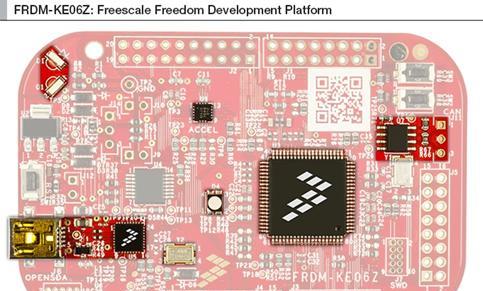
图2. 开发平台FRDM-KE06Z外形图
责任编辑:HanFeng
【免责声明】
1、本文内容、数据、图表等来源于网络引用或其他公开资料,版权归属原作者、原发表出处。若版权所有方对本文的引用持有异议,请联系拍明芯城(marketing@iczoom.com),本方将及时处理。
2、本文的引用仅供读者交流学习使用,不涉及商业目的。
3、本文内容仅代表作者观点,拍明芯城不对内容的准确性、可靠性或完整性提供明示或暗示的保证。读者阅读本文后做出的决定或行为,是基于自主意愿和独立判断做出的,请读者明确相关结果。
4、如需转载本方拥有版权的文章,请联系拍明芯城(marketing@iczoom.com)注明“转载原因”。未经允许私自转载拍明芯城将保留追究其法律责任的权利。
拍明芯城拥有对此声明的最终解释权。
相关资讯
:
基于MC33771主控芯片的新能源锂电池管理系统解决方案

AMIC110 32位Sitara ARM MCU开发方案

基于AMIC110多协议可编程工业通信处理器的32位Sitara ARM MCU开发方案

基于展讯SC9820超低成本LTE芯片平台的儿童智能手表解决方案

基于TI公司的AM437x双照相机参考设计

基于MTK6580芯片的W2智能手表解决方案


 2012- 2022 拍明芯城ICZOOM.com 版权所有 客服热线:400-693-8369 (9:00-18:00)


