


 产品分类
产品分类
基于PowerInt公司的LNK4023D 10W USB充电器参考设计
 135
135
 拍明
拍明
原标题:PowerInt LNK4023D 10W USB充电器参考设计
PowerInt公司的LinkSwitchTM-4系列产品是恒压/恒流初级侧调节(PSR)开关IC,由于不需要光耦合器和此级控制电路从而大大地简化了低功耗CV/CC充电器的设计.器件采用PW/PFM控制器是效率最大化,满足无负载时功耗小于30W的要求,主要用于手机/无绳电话充电器,PDA,MP3/手持音频设备充电器和适配器等.本文介绍了LinkSwitchTM-4系列产品亮点,功能框图, 通用输入10W充电器电路图以及采用LinkSwitchTM-4 LNK4023D 10W CV/CC USB充电器参考设计(RDR-462)主要指标,电路图,材料清单和PCB设计图.
The LinkSwitchTM-4 family of ICs dramatically simplifies low power CV/CC charger design by eliminating an optocoupler and secondary control circuitry. The LinkSwitch-4 family adaptive BJT drive technology uses combined base and emitter switching to boost switching performance and deliver higher efficiency, wider Reverse Bias Safe Operating Area (RBSOA) margin and the flexibility to accommodate a wide range of low cost BJT. The device incorporates a multimode PWM/PFM controller with quasi resonant switch to maximize the efficiency, meet <30 mW no-load and at same time maintain fast transient response greater than 4.3 V with a load change from 0% to 100%.
LinkSwitchTM-4系列产品亮点:
Dramatically Simplifies CV/CC Converters
Eliminates optocoupler and all secondary CV/CC control circuitry
Eliminates all control loop compensation circuitry
Advanced Performance Features
Dynamic base drive technology provides flexibility in choice of BJT transistor by dynamically optimizing BJT switching characteristics Extends RBSOA of BJT
Dramatically reduces sensitivity to BJT gain
Compensates for transformer inductance tolerances
Compensates for input line voltage variations
Compensates for cable voltage drop
Compensates for external component temperature variations
Very accurate IC parameter tolerances using proprietary trimming technology
Frequency up to 65 kHz to reduce transformer size
The minimum peak current is fixed to improve transient load response
Advanced Protection/Safety Features
Single fault output overvoltage and short-circuit
EcoSmart™– Energy Efficient
Meets DoE 6 and CoC V5 2016 via an optimized quasi-resonant switching PWM/PFM control
No-load consumption of <30 mW at 230 VAC input
Green Package
Halogen free and RoHS compliant package
LinkSwitchTM-4系列应用:
Chargers for cell/cordless phones, PDAs, MP3/portable audio devices, adapters, etc.
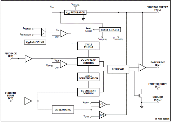
图1. LinkSwitchTM-4系列LNK40x2S功能框图
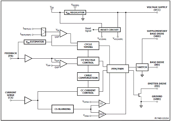
图2. LinkSwitchTM-4系列LNK40x3D功能框图
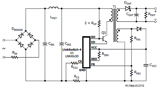
图3. LinkSwitchTM-4系列典型通用输入10W充电器电路图
采用LinkSwitchTM-4 LNK4023D 10W CV/CC USB充电器参考设计(RDR-462)
This document is an engineering report describing a 2 A, 5.0 V USB charger utilizing a device from the LinkSwitch-4 family of ICs. This design is intended to show the high power density and efficiency that is possible due to the high level of integration while still providing exceptional performance.
This document contains the power supply specification, schematic, bill of materials, transformer documentation, printed circuit layout, and performance data.
10W CV/CC USB充电器参考设计(RDR-462)主要特性:
LinkSwitch-4
Primary side regulated (no optocoupler)
±3% CV, ±5% CC regulation
Transient response independent of load timing
<30 mW no-load input power
Cable voltage drop compensation
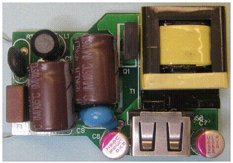
图4. 10W CV/CC USB充电器参考设计(RDR-462)外形图(顶视)

图5. 10W CV/CC USB充电器参考设计(RDR-462)外形图(底视)
10W CV/CC USB充电器参考设计(RDR-462)主要指标:
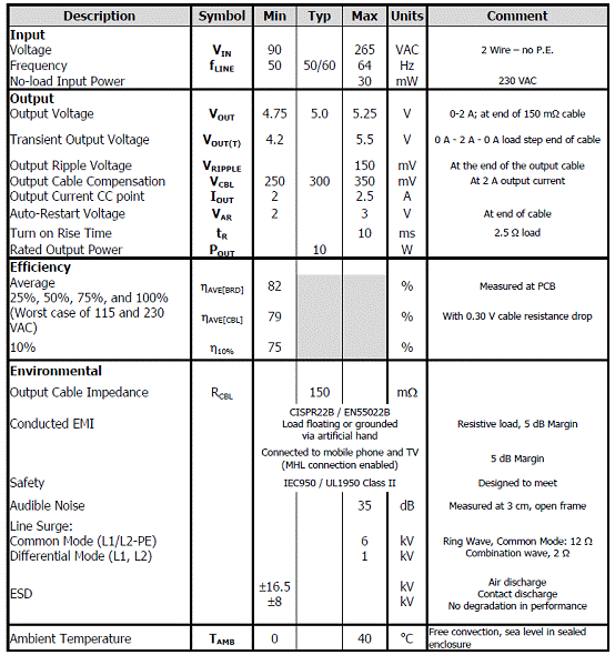
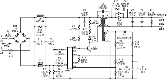
图6. 10W CV/CC USB充电器参考设计(RDR-462)电路图
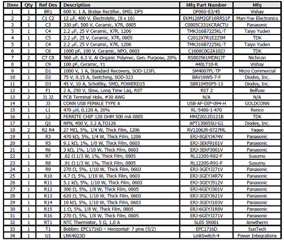
10W CV/CC USB充电器参考设计(RDR-462)材料清单:
责任编辑:HanFeng
【免责声明】
1、本文内容、数据、图表等来源于网络引用或其他公开资料,版权归属原作者、原发表出处。若版权所有方对本文的引用持有异议,请联系拍明芯城(marketing@iczoom.com),本方将及时处理。
2、本文的引用仅供读者交流学习使用,不涉及商业目的。
3、本文内容仅代表作者观点,拍明芯城不对内容的准确性、可靠性或完整性提供明示或暗示的保证。读者阅读本文后做出的决定或行为,是基于自主意愿和独立判断做出的,请读者明确相关结果。
4、如需转载本方拥有版权的文章,请联系拍明芯城(marketing@iczoom.com)注明“转载原因”。未经允许私自转载拍明芯城将保留追究其法律责任的权利。
拍明芯城拥有对此声明的最终解释权。
相关资讯
:
基于MC33771主控芯片的新能源锂电池管理系统解决方案

AMIC110 32位Sitara ARM MCU开发方案

基于AMIC110多协议可编程工业通信处理器的32位Sitara ARM MCU开发方案

基于展讯SC9820超低成本LTE芯片平台的儿童智能手表解决方案

基于TI公司的AM437x双照相机参考设计

基于MTK6580芯片的W2智能手表解决方案


 2012- 2022 拍明芯城ICZOOM.com 版权所有 客服热线:400-693-8369 (9:00-18:00)


