


 产品分类
产品分类
基于Maxim的MAX32600可穿戴医疗保健监视平台
 241
241
 拍明
拍明
原标题:Maxim可穿戴医疗保健监视平台
Maxim公司的可穿戴医疗保健监视平台采用功能强大而非常低功耗的数字MCU,非常低功耗的模拟传感器以及创新的电源和电池管理电路,与通信和用户接口,非常容易开发出可穿戴电子产品如脉搏/心率仪,血氧仪,ECG/EKG,体温计和UV光.本文介绍了可穿戴医疗保健监视平台框图以及系统构成主要元件主要特性和框图,包括电源和电池管理,处理器,传感器和传感器接口,通信和用户接口.
Advances in semiconductor technology have recently enabled extremely low-power battery-powered embedded systems that are so light weight and small that they are wearable. These systems are typically characterized by powerful, very low power microcontrollers that interface to a set of highly sophisticated sensors while communicating information via low-power radio frequency links to external systems.
The combination of powerful, yet very low power digital microcontrollers, very low powered analog body signal sensors, and innovative power and battery management circuits is coenabling the development of the wearable healthcare market.
Body signals have been monitored for many years to provide physicians with useful health diagnoses information. The same monitoring equipment has also been used in high-performance sports applications to help optimize performance. Wearable body signal monitoring products can now provide the same type of information to consumers at much lower price points for both health and performance optimization markets.
For health sensing and monitoring, almost all the signals that are traditionally monitored in a clinical environment can be obtained by a wearable product. These traditional signals include:
Pulse/Heart Rate
Blood Oxygen
Stress
Electrocardiogram (EKG/ECG)
Body Temperature
UV Light (Skin Exposure)
图1 可穿戴医疗保健监视平台框图
一.可穿戴医疗保健监视平台系统构成:
This market is being enabled by high performance and sophisticated ICs. These ICs have been power optimized so they can provide body signal monitoring functionality using small light-weight rechargeable lithium-ion batteries or replaceable nonrechargeable coin-cell type batteries.
While many of these products’main features are implemented via firmware algorithm, the physical design provides a platform to host these features. Once a platform is developed, it can be re-used for an array of different products.
电源和电池管理
Power is a very important aspect of any wearable healthcare platform. This product category must be small and nonintrusive, and so must have a very small, lightweight battery. The total charge available in the battery along with the power dissipation characteristics of the platform determine the product’s usability. Typically, any wearable product would be expected to function over the period of at least a day before requiring recharging. Products with nonrechargeable batteries should have multimonth battery lifetimes.
For devices with rechargeable batteries, the battery management system must include a battery charger and a battery fuel gauge. The battery management system must allow the device to operate while the device is charging.
The power system must be able to regulate voltage from a battery—a voltage source with a declining voltage output. The regulators must be very efficient so as to maximize charge usage, and must also supply the number of rails required by the design. The usable voltage range of a rechargeable Li+ battery ranges from 4.2V to approximately 3.2V. Most wearable products use main power rails that are below the minimum charge of a single-cell Li+ battery, so the main rails within a wearable design are sourced from a step-down regulator. Some functions within a wearable product might require a higher voltage level than is provided by a single-cell battery. To provide these voltage levels the power management function must contain at least one step-up regulator. The number of rails required depends on the device functionality, but for optimum efficiency is it best to minimize the number of required rails.
处理器
Power usage and processing capabilities are the most important selection determinants for a microcontroller for this application. A system partitioning strategy should be used to decide which system functions are best integrated into the microcontroller and which can be handled externally. Because the wearable health devices read body signals, the capabilities of any on-chip data analog circuitry must also be taken into account to ensure they can accurately process low-level body signals.
For a microcontroller, two general low-power strategies are available:
A microcontroller that contains all or most of the needed precision analog circuitry, and A low-cost microcontrollerthat does not have precision analog functionality.
If the lower cost microcontroller option is chosen, the precision signal conversion must take place on external signal processing chains that input sensor signals into the microcontroller digitally. Very small, high-precision and low-power analog circuits are available to support this option.
Many low-power microcontrollers have been recently introduced to the market. The most popular for wearable applications have ARM® architectures that are optimized for low power dissipation. Depending on the processing requirements of the device, the processor will range from 16 bits to 32 bits. The processor will incorporate multiple power consumption modes and the system software will have programmable shut-off and sensor-based wake-up capability.
3.传感器和传感器接口
Many sensors are available to monitor body signals in a wearable device. The sensor technology for obtaining body signals has been available for many years, but only recently have sensors become available that can provide good signals without consuming large amounts of power.
Sensors technology is available to measure the following:
Blood Oxygen
Heart Rate
ECG/EKG
Stress
Temperature
The electrical outputs from these sensors are very small, in the millivolt range. However, many of these popular sensors have been combined with amplification and conversion circuits within a single package so that they output either a higher level analog signal or a serialized digital signal. The interface circuitry for these sensors is engineered for extremely low power operation.
In the case of electrocardiogram sensors, these are essentially physical skin contacts that capture the very small electric field around a skin area and transfer the signal to the EKG signal chain. Low-cost wearable electrocardiograms are limited to between 2 to 3 contact points and do not provide the resolution of higher cost professional ECG/EKG systems that employ from 9 to 11 sensors that are dispersed throughout the body and attached at strategic points.
4.通信
Modern wearable devices will all generally provide a Micro-USB port for mass data transfer, firmware updates, and battery charging. In addition, many wearable wellness products employ a low-power wireless transceiver to transmit and receive data in real time while the device is in use. Wireless transfer allows data transmission to larger display screens or to remote data collection facilities. Low-power Bluetooth is an emerging standard for this purpose. In addition, NFC (near field communication) provides limited-range wireless connectivity that is ideal for short content transfers such as configuration information and logged data retrieval.
Maxim’s MAX66242 secure RFID tag can authenticate a user, thereby accepting communications only from authenticated sources via NFC.
5.用户接口
The user interface for a wearable product will vary based on needed functionality. Low-power design is paramount so the display size is minimized. Depending on the product, the UI will consist of a single-line LCD display with a few control buttons. Products that need to display more information will have a low-power TFT display and most likely include touch-screen capability.
Because processing power has become so cheap and powerful, it is possible that many wearable devices will eventually have a voice command interface.
二.主要元器件
1)健康测量微控制器MAX32600
The MAX32600 microcontroller is based on the industry-standard ARM® Cortex®-M3 32-bit RISC CPU operating at up to 24MHz. It includes 256KB of flash memory, 32KB of SRAM, a 2KB instruction cache, and integrated high-performance analog peripherals.
The MAX32600 comes in 192-ball, 12mm x 12mm CTBGA and 120-ball, 7mm x 7mm CTBGA and 108-ball WLP packages.
In addition to the free tools provided by Maxim, the MAX32600 supports the Embedded Workbench from IAR. The IAR Embedded Workbench® incorporates a compiler, an assembler, a linker, and a debugger into one IDE. It is easy to use, provides advanced and highly-efficient optimization features, and is highly integrated with hardware, RTOS products, and middleware. The IAR Embedded Workbench for ARM is available in several versions, including a product package that is designed specifically for ARM Cortex-M core families.
MAX32600主要特性:
Integrated AFE Enables Precision Wellness Measurements with Minimal Discretes
16-Bit ADC with Input Mux and PGA
Up to 500ksps Conversion Rate
PGA with Gain of 1, 2, 4, and 8 and Bypass Mode
Differential 8:1 or Single-Ended 16:1 Input Mux
Internal Mux Inputs for Measuring VDDA3
Internal or External Voltage Reference
Programmable Buffers for ADC and DACs
Two 12-Bit DACs and Two 8-Bit DACs
Four Operational Amplifiers
Four Low-Power Comparators
Four Uncommitted SPST Analog Switches
Four Ground Switches
Up to Eight 100mA LED Driver Pairs (Sink)
Internal Temperature Sensor
Secure Valuable IP and Data with Robust On-Board Trust Protection Unit
Trust Protection Unit for End-to-End Security
AES Hardware Engine
µMAA for ECDSA and RSA
Hardware PRNG
Fast-Erase SRAM for Secure Key Storage
Industry’s Lowest Overall System Power Increases Battery Life
175μA/MHz Active Power Executing Code from Cache
Less Than 1.0μA Low-Power Mode 0 (LP0) Current
Multiple Power Management Modes to Optimize Power Consumption
Peripheral Clock Control
6-Channel DMA Engine Enables Intelligent Peripheral Operation While Micro is in Sleep Mode
MAX32600应用:
Blood Glucose Metering
Galvanic Skin Response Measurement
Pulse Oximetry Measurement
Wearable Medical Devices
32-Bit ARM Wellness Sensor AFE
MAX32600功能框图
http://www.maximintegrated.com/en/products/digital/microcontrollers/MAX32600.html#popuppdf
2.超低功耗立体声音频codec MAX98091
The MAX98091 is a fully integrated audio codec whose high-performance, ultra-low power consumption and small footprint make it ideal for portable applications.
The device features a highly flexible input scheme with six input pins that can be configured as analog or digital microphone inputs, differential or single-ended line inputs, or as full-scale direct differential inputs. Analog inputs can be routed to the record path ADC or directly to any analog output mixer.
The device accepts master clock frequencies of either 256 x fS or from 10MHz to 60MHz. The digital audio interface supports master or slave mode operation, sample rates from 8kHz to 96kHz, and standard PCM formats such as I²S, left/right-justified, and TDM.
The record/playback paths feature FlexSound® technology DSP. This includes digital gain and filtering, a biquad filter (record), dynamic range control (playback), and a seven band parametric equalizer (playback) that can improve loudspeaker performance by optimizing the frequency response.
The stereo Class D speaker amplifier provides efficient amplification, features low radiated emissions, supports filterless operation, and can drive both 4Ω and 8Ω loads. The DirectDrive® stereo Class H headphone amplifier provides a ground-referenced output eliminating the need for large DC-blocking capacitors. The device also includes a differential receiver (earpiece) amplifier that can be reconfigured as a stereo single-ended line output.
MAX98091简化框图
MAX98091主要特性:
102dB DR Stereo DAC to HP
4.1mW Stereo Playback Power Consumption
99dB DR Stereo ADC
4.5mW Stereo Record Power Consumption
3 Stereo Single-Ended/Differential Analog Microphone/Line Inputs
Two PDM Digital Microphone Inputs
Master Clock Frequencies from 256 x fS to 60MHz
I2S/LJ/RJ/TDM Digital Audio Interface
FlexSound Technology Signal Processing
Record Path Biquad Filter
Playback Path 7-Band Parametric EQ
Playback Path Automatic Level Control
Digital Filtering and Gain/Level Control
Stereo Low EMI Class D Speaker Amplifiers
3.2W/Channel (RL = 4Ω, VSPKVDD = 5V)
1.8W/Channel (RL = 8Ω, VSPKVDD = 5V)
Stereo DirectDrive Class H Headphone Amplifier Jack Detection and Identification
Differential Receiver Amplifier/Stereo Line Output
Extensive Click-and-Pop Reduction Circuitry
RF Immune Analog Inputs and Outputs
Programmable Microphone Bias
I2C Control Interface
56-Bump 0.4mm WLP and 48-Pin 6mm x 6mm x 0.75mm TQFN Packages
MAX98091应用:
Smartphones
Tablets
http://www.maximintegrated.com/en/products/analog/audio/MAX98091.html#popuppdf
3. 低功耗超精度6+3 DoF IMU(惯性测量单元)MAX21100
The MAX21100 is a monolithic 3-axis gyroscope plus 3-axis accelerometer Inertial Measurement Unit (IMU) with integrated 9-axis sensor fusion using proprietary Motion Merging Engine (MME) for handset and tablet applications, game controllers, motion remote controls, and other consumer devices.
The MAX21100 is the industry’s most accurate 6+3 DoF inertial measurement unit available in a 3mm x 3mm x 0.83mm package and capable of working with a supply voltage as low as 1.71V.
The MAX21100 can interface an external magnetometer through a dedicated I²C master.
The internal Motion Merging Engine (MME) can be flexibly configured to get the most suitable accuracy power trade-off.
The MAX21100 is available in a 16-lead plastic land grid array (LGA) package and can operate within a temperature range of -40°C to +85°C.
MAX21100功能框图
MAX21100主要特性:
Fully Integrated, Low Power, Motion Merging Engine Performs Accurate 9DoF Sensor Fusion Using Ultra- Fast, Low Power (50μA) Maxim Proprietary Algorithm Providing:
Quaternion Output
Gravity and Heading Output
High Output Data Rate (ODR) for Accelerometer (Up to 2kHz) and Gyroscope (Up to 8kHz)
Four Selectable Full Scales for Gyroscope (250/500/1000/2000 dps) and Accelerometer (2/4/8/16 g)
I²C Standard (100kHz), Fast (400kHz), and High-Speed (3.4MHz) Serial Interface—10MHz SPI Interface
128 Bytes (64 x 16 Bits) Embedded FIFO with Multiple FIFO Modes
Unique 48-Bit Serial Number as Die ID
5.65mA in Low-Noise Mode and 3.45mA in Eco Mode with MME Active
1.2µA Current Consumption in Power-Down Mode
45ms Turn-On Time from Power-Down and 4ms Turn-On Time from Standby Mode
High Stability Over Temperature and Time: Bias Stability of 4°/hr
High Shock Survivability (10,000g Shock Tolerant)
MAX21100应用:
Appliances and Robotics
GPS and Inertial Navigation Systems
Health and Sports Monitoring
Motion Control with HMI (Human-Machine Interface)
Motion-Based 3D Mice and 3D Remote Controls
Motion-Based Game Controllers
Optical/Electronic Image Stabilizatio
http://www.maximintegrated.com/en/products/analog/sensors-and-sensor-interface/MAX21100.html#popuppdf
4.微型2.1X1.6MM低功耗12位ADC MAX11108
The MAX11108 is a tiny (2.1mm x 1.6mm), 12-bit, compact, high-speed, low-power, successive approximation analog-to-digital converter (ADC). This high-performance ADC includes a high-dynamic range sample-and-hold and a high-speed serial interface. This ADC accepts a full-scale input from 0V to the power supply or to the reference voltage.
The MAX11108 features a single-ended analog input connected to the ADC core. The device also includes a separate supply input for data interface and a dedicated input for reference voltage.
The MAX11108 "communicates" from 1.5V to VDD and operates from a 2.2V to 3.6V supply. The device consumes only 6.6mW at 3Msps and includes full powerdown mode and fast wake-up for optimal power management and a high-speed 3-wire serial interface. The 3-wire serial interface directly connects to SPI/QSPI™/MICROWIRE® devices without external logic.
Excellent dynamic performance, low voltage, low power, ease of use, and extremely small package size make this converter ideal for portable battery-powered dataacquisition applications, and for other applications that demand low-power consumption and minimal space.
The MAX11108 is available in an ultra-TQFN (2.1mm x 1.6mm) package, and operates over the -40°C to +125°C temperature range.

MAX11108应用电路
MAX11108主要特性:
Compact ADC Saves Space
Single-Ended Analog Input 12-Bit Resolution ADC
3Msps Conversion Rate with No Pipeline Delay
73dB SNR
10-Pin, Ultra-TQFN (μDFN), 2.1mm x 1.6mm Package
Low Power Consumption Extends Battery Life
6.6mW at 3Msps
Very Low Power Consumption at 2.5μA/ksps
1.3μA Power-Down Current
2.2V to 3.6V Supply Voltage
Variable I/O Voltage Range of 1.5V to 3.6V Eases Interface to Microcontrollers
SPI-/QSPI-/MICROWIRE-Compatible Serial Interface Directly Connects to 1.5V, 1.8V, 2.5V, or 3V Digital System
MAX11108应用:
Battery-Operated Systems
Communication Systems
Instrument Data Acquisition
Medical Instrumentation
Mobile
Portable Data Logging
http://www.maximintegrated.com/en/products/analog/data-converters/analog-to-digital-converters/MAX11108.html#popuppdf
5.可穿戴充电管理方案MAX14676/14676A
The MAX14676/MAX14676A are battery-charge-management solutions ideal for low-power wearable applications. These devices include a linear battery-charger with a Smart Power Selector™, ModelGauge™ fuel gauge, and several power-optimized peripherals. They feature an ultra-low-power buck regulator with a quiescent current of 900nA (typical) and 74% efficiency with 10μA output.
The battery charger features Smart Power Selector operation, allowing operation with dead battery. It limits input current based on a register setting. If the charger power source is unable to supply the entire system load, the smart power control circuit will supplement the system load with current from the battery.
The MAX14676/MAX14676A embed a Maxim proprietary ModelGauge fuel gauge to provide an accurate estimate of the available capacity for rechargeable lithium batteries.
The MAX14676/MAX14676A include a synchronous high-efficiency step-down converter. The device features a fixed-frequency PWM mode for tighter regulation, and a burst mode for increased efficiency during light-load operation.
The MAX14676/MAX14676A have a boost regulator and three programmable current sinks that can be used to drive a variety of LED configurations. The boost converter is controlled independently from the current sinks, and they can be also used separately.
The MAX14676/MAX14676A feature a power switch controller that allows the device to be turned on and off by a pushbutton. This controller also provides a delayed reset signal and voltage sequencing.
These devices are available in a 42-bump, 0.5mm pitch, 3.497mm x 3.118mm wafer-level package (WLP).
MAX14676/MAX14676A主要特性:
Extend System Use Time Between Battery Charging
1.8V Low-IQ 200mA Buck Regulator
0.9μA (typ) Quiescent Current
Automatic Burst or Forced-PWM Modes
ModelGauge with Accurate State-of-Charge
Easy-to-Implement Li+ Battery Charging
Smart Power Selector
28V Tolerant Input
Thermistor Monitor
Minimize Power-Management Footprint though High Integration
3.2V Low-IQ 100mA LDO
2.0V Always-On 50μA LDO
+5V Safe Output LDO
6.6V Low-IQ 120μA Charge Pump
Support a Wide Variety of Display Options
5V to 17V Output Boost Converter
3-Channel Adjustable High-Voltage Current Sinks
Optimize System Control
Pushbutton to Enable Ultra-Low-Power Mode and Power-On Voltage Sequencing
I2C Control
MAX14676/MAX14676A应用:
Fitness Monitors
GPS Watches
Portable Medical Devices
Wearable Electronics
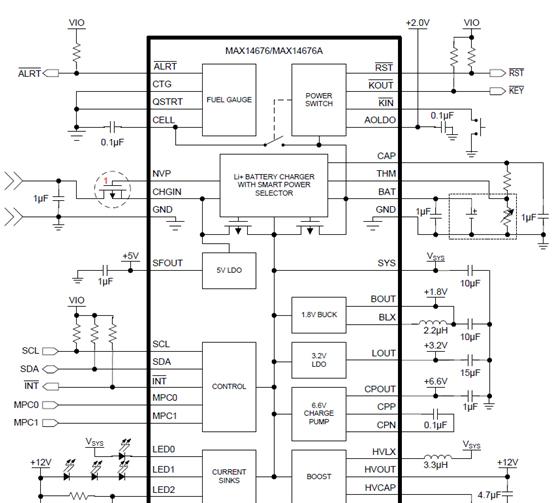
MAX14676/MAX14676A典型应用电路
责任编辑:HanFeng
【免责声明】
1、本文内容、数据、图表等来源于网络引用或其他公开资料,版权归属原作者、原发表出处。若版权所有方对本文的引用持有异议,请联系拍明芯城(marketing@iczoom.com),本方将及时处理。
2、本文的引用仅供读者交流学习使用,不涉及商业目的。
3、本文内容仅代表作者观点,拍明芯城不对内容的准确性、可靠性或完整性提供明示或暗示的保证。读者阅读本文后做出的决定或行为,是基于自主意愿和独立判断做出的,请读者明确相关结果。
4、如需转载本方拥有版权的文章,请联系拍明芯城(marketing@iczoom.com)注明“转载原因”。未经允许私自转载拍明芯城将保留追究其法律责任的权利。
拍明芯城拥有对此声明的最终解释权。
相关资讯
:
基于MC33771主控芯片的新能源锂电池管理系统解决方案

AMIC110 32位Sitara ARM MCU开发方案

基于AMIC110多协议可编程工业通信处理器的32位Sitara ARM MCU开发方案

基于展讯SC9820超低成本LTE芯片平台的儿童智能手表解决方案

基于TI公司的AM437x双照相机参考设计

基于MTK6580芯片的W2智能手表解决方案


 2012- 2022 拍明芯城ICZOOM.com 版权所有 客服热线:400-693-8369 (9:00-18:00)


