


 产品分类
产品分类
基于TI的MSP430F5529 3D打印机解决方案
 321
321
 拍明
拍明
原标题:TI MSP430F5529 3D打印机解决方案
TI公司的MSP430F5529, MSP430F5527, MSP430F5525和MSP430F5521是超低功耗MCU,集成了支持USB 2.0的USB和PHY,四个16位计时器,高性能12位ADC,两个通用USCI,硬件乘法器,DMA,实时时钟模块,具有63个I/O引脚,主要用在模拟和数字传感器系统,数据采集等.本文介绍了MSP430F5529主要特性,框图,以及采用MSP430F5529的3D打印机参考设计主要特性,12V控制器框图,电路图和材料清单.
The Texas Instruments MSP430 family of ultralow-power microcontrollers consists of several devices featuring different sets of peripherals targeted for various applications. The architecture, combined with extensive low-power modes, is optimized to achieve extended battery life in portable measurement applications. The device features a powerful 16-bit RISC CPU, 16-bit registers, and constant generators that contribute to maximum code efficiency. The digitally controlled oscillator (DCO) allows wake-up from low-power modes to active mode in 3.5 µs (typical).
The MSP430F5529, MSP430F5527, MSP430F5525, and MSP430F5521 are microcontroller configurations with integrated USB and PHY supporting USB 2.0, four 16-bit timers, a high-performance 12-bit analog-to-digital converter (ADC), two universal serial communication interfaces (USCI), hardware multiplier, DMA, real-time clock module with alarm capabilities, and 63 I/O pins. The MSP430F5528, MSP430F5526, MSP430F5524, and MSP430F5522 include all of these peripherals but have 47 I/O pins.
The MSP430F5519, MSP430F5517, and MSP430F5515 are microcontroller configurations with integrated USB and PHY supporting USB 2.0, four 16-bit timers, two universal serial communication interfaces (USCI), hardware multiplier, DMA, real time clock module with alarm capabilities, and 63 I/O pins. The MSP430F5514 and MSP430FF5513 include all of these peripherals but have 47 I/O pins.
Typical applications include analog and digital sensor systems, data loggers, and others that require connectivity to various USB hosts.
MSP430F5529主要特性:
Low Supply-Voltage Range: 3.6 V Down to 1.8 V
Ultralow Power Consumption
Active Mode (AM):All System Clocks Active290 µA/MHz at 8 MHz, 3.0 V, Flash Program Execution (Typical)150 µA/MHz at 8 MHz, 3.0 V, RAM Program Execution (Typical)
Standby Mode (LPM3):Real-Time Clock With Crystal, Watchdog, and Supply Supervisor Operational, Full RAM Retention, Fast Wake-Up:1.9 µA at 2.2 V, 2.1 µA at 3.0 V(Typical)Low-Power Oscillator (VLO), General-Purpose Counter, Watchdog, and Supply Supervisor Operational, Full RAM Retention, Fast Wake-Up:1.4 µA at 3.0 V (Typical)
Off Mode (LPM4):Full RAM Retention, Supply Supervisor Operational, Fast Wake-Up:1.1 µA at 3.0 V (Typical)
Shutdown Mode (LPM4.5):0.18 µA at 3.0 V (Typical)
Wake-Up From Standby Mode in 3.5 µs (Typical)
16-Bit RISC Architecture, Extended Memory, up to 25-MHz System Clock
Flexible Power Management System
Fully Integrated LDO With Programmable Regulated Core Supply Voltage
Supply Voltage Supervision, Monitoring, and Brownout
Unified Clock System
FLL Control Loop for Frequency Stabilization
Low-Power Low-Frequency Internal Clock Source (VLO)
Low-Frequency Trimmed Internal Reference Source (REFO)
32-kHz Watch Crystals (XT1)
High-Frequency Crystals up to 32 MHz (XT2)
16-Bit Timer TA0, Timer_AWith Five Capture/Compare Registers
16-Bit Timer TA1, Timer_AWith Three Capture/Compare Registers
16-Bit Timer TA2, Timer_AWith Three Capture/Compare Registers
16-Bit Timer TB0, Timer_BWith Seven Capture/Compare Shadow Registers
Two Universal Serial Communication Interfaces
USCI_A0 and USCI_A1 Each Support: Enhanced UART Supports Auto-Baudrate Detection, IrDA Encoder and Decoder, Synchronous SPI
USCI_B0 and USCI_B1 Each Support: I2CTM, Synchronous SPI
Full-Speed Universal Serial Bus (USB)
Integrated USB-PHY
Integrated 3.3-V and 1.8-V USB Power System
Integrated USB-PLL
Eight Input, Eight Output Endpoints
12-Bit Analog-to-Digital (A/D) Converter (MSP430F552x Only) With Internal Reference, Sample-and-Hold, and Autoscan Feature
Comparator
Hardware Multiplier Supporting 32-Bit Operations
Serial Onboard Programming, No External Programming Voltage Needed
Three Channel Internal DMA
Basic Timer With Real-Time Clock Feature
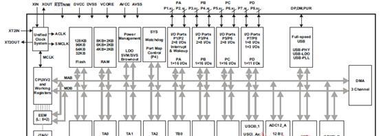
图1。MSP430F5529框图
3D打印机参考设计
此设计是用于控制基于单个挤出机的 3 轴 3D 打印机的完整系统。该系统由 MSP430F5529 LaunchPad进行管理,并利用 DRV8846 实现精度步进电机控制。CSD18534Q5A 用作温床加热器、挤出机加热器和冷却风扇的低侧开关。DRV5033 霍尔传感器充当非接触式限位开关。
3D打印机参考设计特性:
包含 MCU、步进驱动器、加热器输出、传感器输入和 SD 卡槽的完整 3D 打印机控制器。
使用 DRV8846 自适应衰减实现精确的步进电机电流调节
霍尔传感器限位开关不受污染物影响且永不磨损
来自 CSD18534Q5A 的高电流加热器输出,导通阻抗低至 7.8 mΩ
由单个 12V 电源供电
系统已经过全面测试和实践检验
主要的TI 器件:
DRV5033
DRV8846
CSD18534Q5A
MSP430F5529
UA78M33

图2。3D打印机参考设计外形图
The 3D Printer Controller (12V) Reference Design is a complete system for controlling common 3-axis, single extruder based 3D printers. The controller runs off of a 12 V power supply for the steppermotor drivers, hot bed heater, extruder heater, and fan driver. The supply is regulated down for 3.3 V inorder to supply the microcontroller and sensors. Data in this report was taken running the controller at12 V and demonstrates the various capabilities of the design.
This design utilizes the MSP430F5529 LaunchPad (mother board) in combination with a 3D Printerspecific BoosterPack (daughter board) to provide the system solution. The MSP430F5529microcontroller is used to control the stepper motor drivers and power switches. The microcontrollercan accept commands from either a USB connection or onboard micro-SD card. The four DRV8846’sare used to drive the axis and extruder stepper motors. The three CSD18534Q5A are used as thepower switches for the hot bed, hot end, and fan. The UA78M33CDCY regulates the input supply downto the 3.3 V supply for the microcontroller and sensors. The controller can take in signals from up to sixlimit switches and two thermistors. The reference design utilizes the DRV5033 as a contactless limitswitch to sense the magnets that are mounted onto each axis.
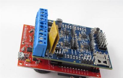
图3。12V 3D打印机控制器(12V)外形图
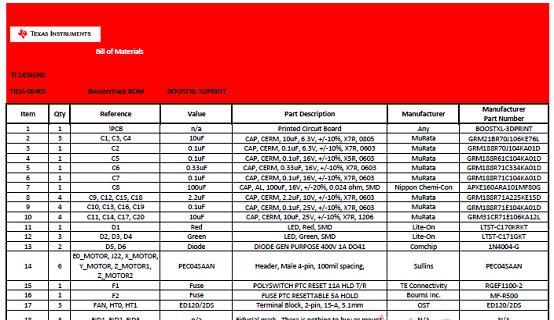
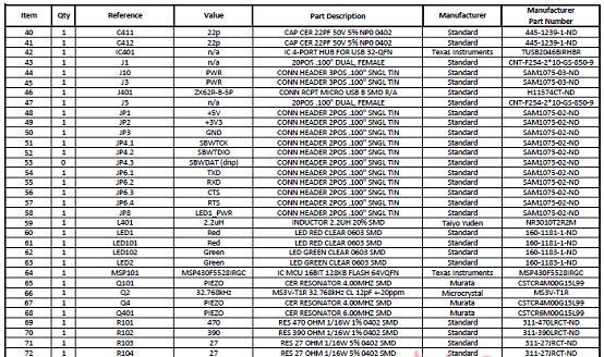
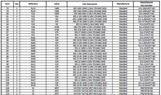
12V 3D打印机控制器材料清单:


责任编辑:HanFeng
【免责声明】
1、本文内容、数据、图表等来源于网络引用或其他公开资料,版权归属原作者、原发表出处。若版权所有方对本文的引用持有异议,请联系拍明芯城(marketing@iczoom.com),本方将及时处理。
2、本文的引用仅供读者交流学习使用,不涉及商业目的。
3、本文内容仅代表作者观点,拍明芯城不对内容的准确性、可靠性或完整性提供明示或暗示的保证。读者阅读本文后做出的决定或行为,是基于自主意愿和独立判断做出的,请读者明确相关结果。
4、如需转载本方拥有版权的文章,请联系拍明芯城(marketing@iczoom.com)注明“转载原因”。未经允许私自转载拍明芯城将保留追究其法律责任的权利。
拍明芯城拥有对此声明的最终解释权。
相关资讯
:
基于MC33771主控芯片的新能源锂电池管理系统解决方案

AMIC110 32位Sitara ARM MCU开发方案

基于AMIC110多协议可编程工业通信处理器的32位Sitara ARM MCU开发方案

基于展讯SC9820超低成本LTE芯片平台的儿童智能手表解决方案

基于TI公司的AM437x双照相机参考设计

基于MTK6580芯片的W2智能手表解决方案


 2012- 2022 拍明芯城ICZOOM.com 版权所有 客服热线:400-693-8369 (9:00-18:00)


