


 产品分类
产品分类
Freescale MCF51AG128三相BLDC马达控制设计方案
 110
110
 拍明
拍明
原标题:Freescale MCF51AG128三相BLDC马达控制设计方案
freescale公司的MCF51AG128是32位ColdFire微控制器,内核提供50 MHz的内核速度和25 MHz的总线速度,提供带有直接存储器访问(DMA)和iEvent模块,提供带有直接存储器访问(DMA)和iEvent模块配备与其先进的三相电机控制的需求相符的外设组合和系统安全和完整性功能.主要用在智能家电和工业应用.本文介绍了MCF51AG128主要特性和框图,以及采用MCF51AG128无传感器三相BLDC马达演示板特性,框图,软件流程图和电路图.
The MCF51AG128 is a member of the ColdFire® family of32-bit variable-length reduced instruction set (RISC)microcontroller. This document provides an overview of theMCF51AG128 series MCUs, focusing on its highlyintegrated and diverse feature set.
The MCF51AG128 derivative are low-cost, low-power, andhigh-performance 32-bit ColdFire V1 microcontroller units(MCUs) designed for industrial and appliance applications. Itis an ideal upgrade for designs based on the MC9S08AC128series of 8-bit microcontrollers.
MCF51AG128主要特性:
• 32-bit Version 1 ColdFire® central processor unit (CPU)
– Up to 50.33 MHz ColdFire CPU from 2.7 V to 5.5 V
– Provide 0.94 Dhrystone 2.1 DMIPS per MHzperformance when running from internal RAM (0.76
DMIPS per MHz when running from flash)
– Implements Coldfire Instruction Set Revision C(ISA_C)
• On-chip memory
– Up to 128 KB flash memory read/program/erase overfull operating voltage and temperature
– Up to 16 KB random access memory (RAM)
– Security circuitry to prevent unauthorized access toRAM and flash contents
• Power-Saving Modes
– Three ultra-low power stop modes and reduced powerwait mode
– Peripheral clock enable register can disable clocks tounused modules, thereby reducing currents
• System Protection
– Advanced independent clocked watchdog (WDOG)with features like, robust refresh mechanism, windowedmode, high granulation timeout, fast test of timeout, andalways forces a reset
– Additional external watchdog monitor (EWM) to helpreset external circuits
– Low-voltage detection with reset or interrupt
– Separate low voltage warning with selectable trip points
– Illegal opcode and illegal address detection with reset
– Flash block protection for each array to preventaccidental write/erasure
– Hardware CRC module to support fast cyclicredundancy checks
• Debug Support
– Single-wire back ground debug interface
– Real-time debug support, with six hardware breakpoints(4 PC, 1 address pair and 1 data) that can be configuredinto a 1- or 2-level trigger
– On-chip trace buffer provides programmable start/stoprecording conditions
– Support for real-time program (and optional partial data)trace using the debug visibility bus
• DMA Controller
– Four independently programmable DMA channelsprovide the means to directly transfer data betweensystem memory and I/O peripherals
– DMA enabled peripherals include IIC, SCI, SPI, FTM,HSCMP, ADC, RTC, and eGPIO, and the DMA requestfrom these peripherals can be configured as DMAsource or as an iEvent input
• CF1_INTC
– Support of 44 peripheral I/O interrupt requests and sevensoftware (one per level) interrupt requests
– Fixed association between interrupt request source, leveland priority, up to two requests can be remapped to thehighest maskable level and priority
– Unique vector number for each interrupt source
– Support for service routine interrupt acknowledge(software IACK) read cycles for improved system
performance
– Ability to mask any individual or all interrupt sources
• System Clock Sources
– Oscillator (XOSC) — Loop-control pierce oscillator; crystal or ceramic resonator range of 31.25 kHz to 38.4 kHz or 1MHz to 16 MHz
– Internal Clock Source (ICS) — Frequency-locked-loop (FLL) controlled by internal or external eference; trimmableinternal reference allows 0.2% resolution and 2% deviation (1% across 0 to 70 ºC)
• Peripherals
– ADC — 24 analog inputs with 12 bits resolution; output formatted in 12-, 10- or 8-bit right-justified format; single orcontinuous conversion (automatic return to idle after single conversion); interrupt or DMA request when conversioncomplete; operation in low-power modes for lower noise operation; asynchronous clock source for lower noise operation;selectable asynchronous hardware conversion triggers from RTC, PDB, or iEvent; dual samples based on hardwaretriggers during ping-pong mode; on-chip temperature sensor
– PDB — 16-bit of resolution with prescaler; seven possible trigger events input; positive transition of trigger event signalinitiates the counter; support continuous trigger or single shot, bypass mode; supports two triggered delay outputs or ORedtogether; pulsed output could be used for HSCMP windowing signal
– iEvent — User programmable combinational boolean output using the four selected iEvent input channels for use asinterrupt requests, DMA transfer requests, or hardware triggers
– FTM — Two 6-channel flexible timer/PWM modules with DMA request option; deadtime insertion is available for eachcomplementary channel pair; channels operate as pairs with equal outputs, pairs with complimentary outputs orindependent channels (with independent outputs); 16-bit free-running counter; the load of the FTM registers which havewrite buffer can be synchronized; write protection for critical registers; backwards compatible with TPM
– TPM — 16-bit free-running or modulo up/down count operation; two channels, each channel may be input capture, outputcompare, or edge-aligned PWM; one interrupt per channel plus terminal count interrupt
– CRC — High speed hardware CRC generator circuit using 16-bit shift register; CRC16-CCITT compliancy with x16 + x12+ x5 + 1 polynomial; error detection for all single, double, odd, and most multi-bit errors; programmable initial seed value
– HSCMP — Two analog comparators with selectable interrupt on rising edge, falling edge, or either edges of comparatoroutput; the positive and negative inputs of the comparator are both driven from 4-to-1 muxes; programmable voltagereference from two internal DACs; support DMA transfer
– IIC — Compatible with IIC bus standard and SMBus version 2 features; up to 100 kbps with maximum bus loading;multi-master operation; software programmable for one of 64 different serial clock frequencies; programmable slaveaddress and glitch input filter; interrupt driven byte-by-byte data transfer; arbitration lost interrupt with automatic modeswitching from master to slave; calling address identification interrupt; bus busy detection; broadcast and 10-bit addressextension; address matching causes wake-up when MCU is in Stop3 mode; DMA support
– SCI — Two serial communications interface modules with optional 13-bit break; full-duplex, standard non-return-to-zero(NRZ) format; double-buffered transmitter and receiver with separate enables; 13-bit baud rate selection with /32fractional divide; interrupt-driven or polled operation; hardware parity generation and checking; programmable 8-bit or9-bit character length; receiver wakeup by idle-line or address-mark; address match feature in receiver to reduceaddress-mark wakeup ISR overhead; 1/16 bit-time noise detection; DMA transmission for both transmit and receive
– SPI — Two serial peripheral interfaces with full-duplex or single-wire bidirectional option; double-buffered transmitterand receiver; master or slave mode operation; selectable MSB-first or LSB-first shifting; 8-bit or 16-bit data modes;programmable transmit bit rate; receive data buffer hardware match feature; DMA transmission for transmit and receive
• Input/Output
– Up to 69 GPIOs and one Input-only pin
– Interrupt or DMA request with selectable polarity on all input pins
– Programmable glitch filter, hysteresis and configurable pull up/down device on all input pins
– Configurable slew rate and drive strength on all output pins
– Independent pin value register to read logic level on digital pin
– Up to 16 rapid general purpose I/O (RGPIO) pins connected to the processor’s local 32-bit platform bus with set, clear,and faster toggle functionality

图1. MCF51AG128系列MCU框图
采用MCF51AG128无传感器三相BLDC马达演示板
3-Phase BLDC Sensorless Control using MCF51AG128
This design reference manual describes the design of a sensorless 3-phase Brushless DC (BLDC) motordrive based on Freescale’s 32-bit MCF51AG128 control device.
BLDC motors are very popular in a wide application area. The BLDC motor lacks a commutator and istherefore more reliable than the DC motor. The BLDC motor also has advantages when compared to anAC induction motor. Because it achieves a higher efficiency by generating the rotor magnetic flux withrotor magnets, a BLDC motor is used in high-end white goods (such as refrigerators, washing machines,dishwashers), high-end pumps, fans and in other appliances which require a high reliability and efficiency.
The concept of the application is a speed and torque closed-loop BLDC drive using a sensorless BEMFzero crossing technique. It serves as an example of a BLDC motor control design using a FreescaleColdFire V1 Family MCU.
This reference design includes basic motor theory, system design concept, hardware implementation, andsoftware design, including the FreeMASTER software visualization tool.
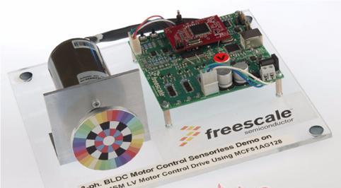
图2.采用MCF51AG128无传感器三相BLDC马达演示板外形图
The motor control system is designed to drive a 3-phase Brushless DC Motor (BLDC Motor) in acombined speed/torque closed-loop. The application meets the following performance specifications:
• Sensorless Brushless DC Motor Control by Back-EMF zero-crossing sensing
• Targeted at the MCF51AGx platform
• Running on a low voltage (24 V) 3-phase Motor Control Drive board
• Control technique incorporates:
— Sensorless control with the combined speed/torque closed-loop
— Using an ADC for zero-crossing sensing
— Rotation in both directions
— Full 4-quadrant operation
— Start from any motor position with rotor alignment
— Manual interface (Direction switch, Up/Down push button control)
— FreeMASTER software control interface (motor run/stop, speed/torque set-up)
— FreeMASTER software remote monitor
— MCU initialization is done by Device Initialization tool (part of Processor Expert)
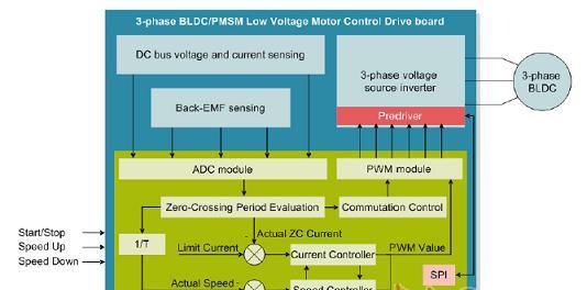
图3.三相BLDC/PMSM低压马达驱动板框图
责任编辑:HanFeng
【免责声明】
1、本文内容、数据、图表等来源于网络引用或其他公开资料,版权归属原作者、原发表出处。若版权所有方对本文的引用持有异议,请联系拍明芯城(marketing@iczoom.com),本方将及时处理。
2、本文的引用仅供读者交流学习使用,不涉及商业目的。
3、本文内容仅代表作者观点,拍明芯城不对内容的准确性、可靠性或完整性提供明示或暗示的保证。读者阅读本文后做出的决定或行为,是基于自主意愿和独立判断做出的,请读者明确相关结果。
4、如需转载本方拥有版权的文章,请联系拍明芯城(marketing@iczoom.com)注明“转载原因”。未经允许私自转载拍明芯城将保留追究其法律责任的权利。
拍明芯城拥有对此声明的最终解释权。
相关资讯
:
基于MC33771主控芯片的新能源锂电池管理系统解决方案

AMIC110 32位Sitara ARM MCU开发方案

基于AMIC110多协议可编程工业通信处理器的32位Sitara ARM MCU开发方案

基于展讯SC9820超低成本LTE芯片平台的儿童智能手表解决方案

基于TI公司的AM437x双照相机参考设计

基于MTK6580芯片的W2智能手表解决方案


 2012- 2022 拍明芯城ICZOOM.com 版权所有 客服热线:400-693-8369 (9:00-18:00)


