基于TI TMS320LC542数字信号处理器的TCS2315 GPRS手机解决方案
 202
202
 拍明
拍明
原标题:TCS2315 GPRS手机解决方案
TI 公司的TCS2315 GPRS手机解决方案是第三代基于GSM的超低成本手机,采用先进的65-nm工艺技术,在单片上集成了TMS320C54x™ DSP 和ARM7核以及数字RF DRP™ 技术,具有高性能以及强大的功能如GPRS功能,内置的VGA功能支持JPEG编译码和先进的图像功能如旋转和变焦等,用来在PC和手机间数据传输的USB连接以及蓝牙连接等,主要适合印度,中国,俄罗斯和巴西等国市场。本文介绍了TCS2315 GPRS手机解决方案的主要性能特点和指标以及方框图。
TIs third-generation GSM-based solutions for the Ultra Low-Cost (ULC) Handsets
Leveraging an advanced 65-nm process with TMS320C54x™ DSP and ARM7 cores in the same package, the TCS2315 GPRS solution integrates TIs breakthrough digital RF DRP™ technology to offer the most compelling user experience in Ultra Low-Cost (ULC) handsets. Part of the LoCosto ULC family, the TCS2315 enables handsets with high performance, robust functionality and innovative form factors in the most price-sensitive handsets. Ideal for emerging markets such as India, China, Russia and Brazil where the next billion subscribers will come from, the scalability and flexibility of the TCS2315 LoCosto ULC GPRS chipset also allow it to be deployed in enhanced handsets for value-conscious segments in more mature markets.
Software portability from one generation of LoCosto solution to the next gives manufacturers and operators the ability to rapidly and cost-effectively differentiate handsets and service offerings for both emerging and mature markets, crossing over regional borders, language barriers and subscriber requirements.
A set of enhanced capabilities are now possible in ULC handsets, such as a relatively high-resolution color display without requiring additional external SRAM, VGA camera support, MP3 playback and mass storage (SD/MMC), USB and Bluetooth® connectivity, high-end full duplex voice quality, a MIDI player with 32 polyphonics, MP3 and polyphonic ringers, longer talk time and standby time, stereo FM radio connectivity, USB charging, handsfree speakerphone operation, vibration ringer, headset support and other functionality.
Equipped with TIs scalable and hardware-based M-Shield™ security technology, a TCS2315 handset offers ironclad protection of the owners personal information. M-Shield also prevents the unlocking of the handsets SIMlock code, defeating attempts to switch networks. High-value content and IP can be fully protected from tampering, piracy and malicious attacks.
Innovative user form factors such as ultra-slim, clamshell and candybar handsets are possible because of the reduced component count and PCB board space requirements brought about by the smaller 65-nm process node, increased integration, and advanced packaging technologies for a single-chip solution. In addition, a smaller PCB area requirement allows a handset to support larger batteries for a longer battery life enabling extended standby and talk times. The superb full-duplex quality of voice service of the
“LoCosto ULC” solutions are comparable to more expensive handsets. In fact, the voice loudness on both ends of a call can be improved by 7 dB or practically twice as loud. Moreover, voice chopping and double talk are reduced dramatically, making handsets based on the TCS2305 and TCS2315 solutions very effective in handsfree applications and noisy environments, characteristic of densely populated emerging markets. The TCS2305 and TCS2315 also offer SMS text messaging, a Universal Subscriber Identity
Module (USIM) interface for SIM cards and support for a standard keypad and joy stick.
Lowering the power dissipation in the advanced “LoCosto ULC” solutions extend the battery life of a handset, lengthening the standby and talk times for users. “LoCosto ULC” single-chip platform integrates power management functions for best-in-class power consumption levels and supports USB charging for universal and easy charger access. This eliminates the need to supply a charger with the phone (saving costs) and minimizes electronic waste from incompatible or obsolete chargers.
Concerns over the security of wireless handsets are completely mitigated by TI’s scalable and hardware-based M-Shield™ technology. The “LoCosto ULC” solutions take advantage of M-Shield technology to safeguard not just the handset owner’s sensitive personal information, but it also defeats malicious attempts to unlock the handset’s SIMlock code. Cracking the SIMlock code can increase subscriber churn because users are able to switch a handset that had been locked to one network to another provider’s network. To reduce phone theft and protect the service provider’s investment insubsidized handsets, TI’s M-Shield technology secures the contents of flash memory,
including boot code, and provides robust SIMLock and handset’s International Mobile Equipment Identity (IMEI) protection. This level of protection is simply not possible with software-based security systems.
TI’s M-Shield security technology includes secure read-only memory (ROM), unique hardware-based public keys, and other protection measures to safeguard valuable information, data and software stored on a handset, including sensitive personal information of handset owners as well as the device’s boot code and other critical firmware modules provided by the handset manufacturer. The investment handset manufacturers have made in developing software and other intellectual property (IP) is protected against piracy and the handset itself is safeguarded against malicious attackers attempting to install viruses, worms and other unwanted software on the device.
Fabricating the “LoCosto ULC” solutions with 65-nm process technology as well as several other chip- and system-level cost optimization techniques all contribute to the device’s sustainable ULC characteristics. For example, the electronic bill of materials (eBOM) for an entry-level ULC handset is reduced by up to 25 percent with the “LoCosto ULC” solutions compared with the previous generation. Additionally, fabricating the chip at a smaller process node means that the chip itself is substantially smaller. This, along with component reduction, reduces the size of a handset’s PCB, lowering the manufacturing cost of the cell phone. Integration of the power management with the digital baseband into a single chip also yields reduction in the modem PCB area.

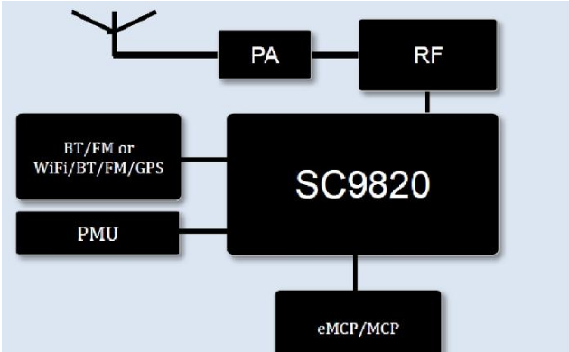
图1.TCS2315 “LoCosto ULC“ GPRS手机方框图
【TMS320LC542 数字信号处理器】
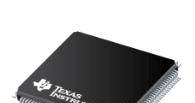
描述
The TMS320C54x, TMS320LC54x, and TMS320VC54x fixed-point, digital signal processor (DSP) families (hereafter referred to as the ’54x unless otherwise specified) are based on an advanced modified Harvard architecture that has one program memory bus and three data memory buses. These processors also provide an arithmetic logic unit (ALU) that has a high degree of parallelism, application-specific hardware logic, on-chip memory, and additional on-chip peripherals. These DSP families also provide a highly specialized instruction set, which is the basis of the operational flexibility and speed of these DSPs.
Separate program and data spaces allow simultaneous access to program instructions and data, providing the high degree of parallelism. Two reads and one write operation can be performed in a single cycle. Instructions with parallel store and application-specific instructions can fully utilize this architecture. In addition, data can be transferred between data and program spaces. Such parallelism supports a powerful set of arithmetic, logic, and bit-manipulation operations that can all be performed in a single machine cycle. In addition, the ’C54x, ’LC54x, and ’VC54x versions include the control mechanisms to manage interrupts, repeated operations, and function calls.
特性
Advanced Multibus Architecture With Three Separate 16-Bit Data Memory Buses and One Program Memory Bus
40-Bit Arithmetic Logic Unit (ALU) Including a 40-Bit Barrel Shifter and Two Independent 40-Bit Accumulators
17- × 17-Bit Parallel Multiplier Coupled to a 40-Bit Dedicated Adder for Non-Pipelined Single-Cycle Multiply/Accumulate (MAC) Operation
Compare, Select, and Store Unit (CSSU) for the Add/Compare Selection of the Viterbi Operator
Exponent Encoder to Compute an Exponent Value of a 40-Bit Accumulator Value in a Single Cycle
Two Address Generators With Eight Auxiliary Registers and Two Auxiliary Register Arithmetic Units (ARAUs)
Data Bus With a Bus Holder Feature
Address Bus With a Bus Holder Feature (’548 and ’549 Only)
Extended Addressing Mode for 8M × 16-Bit Maximum Addressable External Program Space (’548 and ’549 Only)
192K × 16-Bit Maximum Addressable Memory Space (64K Words Program, 64K Words Data, and 64K Words I/O)
On-Chip ROM with Some Configurable to Program/Data Memory
Dual-Access On-Chip RAM
Single-Access On-Chip RAM (’548/’549)
Single-Instruction Repeat and Block-Repeat Operations for Program Code
Block-Memory-Move Instructions for Better Program and Data Management
Instructions With a 32-Bit Long Word Operand
Instructions With Two- or Three-Operand Reads
Arithmetic Instructions With Parallel Store and Parallel Load
Conditional Store Instructions
Fast Return From Interrupt
On-Chip Peripherals
Software-Programmable Wait-State Generator and Programmable Bank Switching
On-Chip Phase-Locked Loop (PLL) Clock Generator With Internal Oscillator or External Clock Source
Full-Duplex Serial Port to Support 8- or 16-Bit Transfers (’541, ’LC545, and ’LC546 Only)
Time-Division Multiplexed (TDM) Serial Port (’542, ’543, ’548, and ’549 Only)
Buffered Serial Port (BSP) (’542, ’543, ’LC545, ’LC546, ’548, and ’549 Only)
8-Bit Parallel Host-Port Interface (HPI) (’542, ’LC545, ’548, and ’549)
One 16-Bit Timer
External-Input/Output (XIO) Off Control to Disable the External Data Bus, Address Bus and Control Signals
Power Consumption Control With IDLE1, IDLE2, and IDLE3 Instructions With Power-Down Modes
CLKOUT Off Control to Disable CLKOUT
On-Chip Scan-Based Emulation Logic, IEEE Std 1149.1 (JTAG) Boundary Scan Logic
25-ns Single-Cycle Fixed-Point Instruction Execution Time [40 MIPS] for 5-V Power Supply (’C541 and ’C542 Only)
20-ns and 25-ns Single-Cycle Fixed-Point Instruction Execution Time (50 MIPS and 40 MIPS) for 3.3-V PowerSupply (’LC54x)
15-ns Single-Cycle Fixed-Point Instruction Execution Time (66 MIPS) for 3.3-V Power Supply (’LC54xA, ’548, ’LC549)
12.5-ns Single-Cycle Fixed-Point Instruction Execution Time (80 MIPS) for 3.3-V Power Supply (’LC548, ’LC549)
10-ns and 8.3-ns Single-Cycle Fixed-Point Instruction Execution Time (100 and 120 MIPS) for 3.3-V Power Supply (2.5-V Core) (’VC549)
责任编辑:David
【免责声明】
1、本文内容、数据、图表等来源于网络引用或其他公开资料,版权归属原作者、原发表出处。若版权所有方对本文的引用持有异议,请联系拍明芯城(marketing@iczoom.com),本方将及时处理。
2、本文的引用仅供读者交流学习使用,不涉及商业目的。
3、本文内容仅代表作者观点,拍明芯城不对内容的准确性、可靠性或完整性提供明示或暗示的保证。读者阅读本文后做出的决定或行为,是基于自主意愿和独立判断做出的,请读者明确相关结果。
4、如需转载本方拥有版权的文章,请联系拍明芯城(marketing@iczoom.com)注明“转载原因”。未经允许私自转载拍明芯城将保留追究其法律责任的权利。
拍明芯城拥有对此声明的最终解释权。


 产品分类
产品分类




 2012- 2022 拍明芯城ICZOOM.com 版权所有 客服热线:400-693-8369 (9:00-18:00)


