


 产品分类
产品分类
晶心科技(Andes)推出新一代处理器AndesCore N820
 350
350
 拍明
拍明
随著物联网(Internet of Thing)的应用日趋智慧化及複杂化,对于处理器高效能的需求也日益提升。亚洲首家以原创性32位元微处理器IP与系统晶片设计平台为主要产品的晶心科技(Andes),基于AndesCore™ N8家族第一代处理器的成功,近期推出的家族第二代处理器N820。除保有第一代低功耗小面积的优点外,N820在执行效能与程式码大小上都有更佳的表现。N820涵盖第一代产品的应用领域,如触控萤幕控制器、医疗装置、电脑週边、白色家电及手持式装置等,同时还可进一步应用在高阶感测器中枢(Sensor Hub)、智慧电表、无线传输及工业控制等领域。
晶心AndesCore™ N820处理器具有1.82 DMIPS/MHz的高效能,在90nm LP製程呈现11.4 uW/MHz低动态功耗(Dynamic Power),达到121DMIPS/mW的能源效率(Power Efficiency),是业界领先厂商同级产品的2.5倍。在28HPM的先进製程动态功耗则只有3.1uW/MHz。此优越的性能可以充分支援需要低功耗和高效能的各项应用。晶心AndesCore™ N820处理器使用AndeStar™ V3m+指令集架构,并且结合多种突破性的技术,可以令晶片供应商达到最佳的系统效能,最小的程式码(Code Size),和最小的能量消耗(Power Consumption)。 除此之外,N820的电源管理指令及提供业界普遍使用的AHB-lite或APB汇流排让客户可以在最短的时间直接无接轨的提升下一代的晶片效能。除此之外,N820提供区域记忆体(Local memory)的配置,可以提升存取指令及资料的效率。针对SoC常用非挥发性但速度较慢功耗较高的Flash记忆体,N820的指令区域记忆体介面可连接选购的FlashFetch IP,以caching及prefetching技术大幅提高Flash指令存取的效率以及降低整体的功耗。而其SPI Flash控制器支援Execute-in-Place的功能,可以让CPU直接执行位于外部的Flash的程式码。
晶心科技技术长兼研发副总经理 苏泓萌博士表示,相对于第一代N8家族的V3m架构,第二代的N820具有来自新的V3m +架构的先进代码压缩技术,程式代码大小平均减少10%,可帮客户降低SoC成本。N820实现3R2W寄存器端口,分支预测(Branch prediction)和返回位址堆叠(Return address stack)的选项,从而在基准效能上提高15%。除16MB的系统定址空间外,N820增加可应用在较大系统环境的4GB选项,并加入可提高程式可靠度的堆叠溢出及不足(Stack overflow/underflow)的硬体预警机制。整体而言,N820的效能提升开拓新的应用,虽然其总效能稍低于N9家族,但却有1.5倍的最佳能源效率(Power Efficiency) ,基本配置(Base configuration)的面积则仅有N9的25%。因此N820在SoC的成本上更有竞争力。
晶心科技介绍
在短短数年间,由晶心科技提供的AndesCore™ IP 解决方案已成为市场中佼佼者,并且在其客户群中累计有超过17亿颗的芯片出货量。这个令人惊艳的结果来自于晶心科技所坚持的两个原则。首先是我们强调的「能效比」,它可以达到极高的效能,同时保持片上系统(SoC)层的超低功耗。晶心科技的客户会发现,不论所需要效能为何,所有AndesCore™的CPU及外围IP,都能以独有的方式来确保能耗的需求降到最低。

第二个原则是致力于倾听我们的客户和合作伙伴,并提供给他们需要的优质产品。晶心科技的每个新产品,皆是由晶心创新性的研发创意结合客户实际使用经验所产出的,举例而言,我们能够透过高度可配置的RTL及软件支持带给客户相当程度的产品可塑性。为了达到他们的质量要求,我们不仅提供完整的技术文件,还包括实现关键──IP验证的程序。我们的重要客户经验部分源自于我们总部的位置──在台湾的新竹科学工业园区。在这里,我们能够与大量的客户、制造伙伴和频繁地到此地出差或是在这里设有办公室的半导体行业的其他成员进行互动。如果您因为洽谈公事来到台湾,非常欢迎您拜访晶心科技的总部。
晶心科技的所有产品都源自于获得专利的AndeStar™指令集架构(ISA)。这是一个由晶心科技专门研发的类RISC架构,目的是为了实现更高的能效比和降低功耗。AndeStar是新一代的RISC计算架构,有其他ISA架构中所没有的性能和功耗特色。
AndesCore产品范围从小型的微型处理器到高端的MMU多核心处理器,产品一应俱全。MCU类的微处理器通常应用于从8051升级上来的客户,而多核心处理器则应用于速度高于1 GHz的运算,当客户不想使用昂贵的函数库或高耗能的处理器时,AndesCore的高阶处理器成为客户的不二选项。我们通过选用浮点协处理器和DSP指令功能来增强我们的核,同时透过PowerBrake™和FlashFetch™等技术来节省功耗。我们的AndeSight™软件及工具链是绝对一流的,它是基于行业标准的GCC编译器和Eclipse调试器来开发的。我们的质量控制更是首屈一指,晶心拥有超过120个CPU授权客户并且超过10,000个用户使用我们的工具进行程序开发。
即使我们的AndeShape™ SOC外围IP等也都是基于提供「能效比」及低功耗的概念来设计的,使用起来简单可靠。
靠着对能效比以及产品质量的关注,晶心已拓展到许多具备发展潜力的市场,例如:物联网、穿戴式设备、网络、取代8位处理器等。
AndesCore™ Processor
产品与解决方案AndesCore™ Processor
AndesCore™ is made up of a series of high performance 32-bit CPU core families specially designed to target different market segments of today's emerging embedded applications. The small gate count and high power efficiency AndesCore™ 2- and 3-stage N7 and N8 families are the best candidates to replace 8bit/16bit microcomputer in consumer applications. The N7 and N8 also deliver much better power efficiency (DMIPS/mW) than popular competing 32-bit processors. The AndesCore™ 3-stage S8 family supports the Security Extension Micro Profile of AndeStar architecture. It is a secure processor core capable of code and data protection from physical attacks and malicious debugging. The S8 family is specially suitable for smart card and secure card applications. The AndesCore E8 family targets Internet of Things (IoT) applications with the unique Andes Custom Extension™ (ACE) on a power-efficient compact embedded controller. The E8's unique ACE environment enables designers to specify the architectural element that makes the core ideal for IoT applications. With Andes' Custom-OPtimized Instruction deveLOpment Tools (COPILOT), designers can create custom instructions that differentiate their design from competitive offerings, which are based on standard instruction set processors. By adding special instructions, not easily discoverable by hackers, ACE also provides stronger security to a design.
The 5-stage AndesCore™ N9 family, with its cost-effective features, is ideal for embedded controller market such as general-purpose MCU, automotive control, and storage. The designers can configure certain parameters of the N9 to adjust the CPU's size, power, and performance. The highly performance-efficient AndesCore™ N10 family is ideal for applications ranging from consumer media players and smart glasses all the way to touch panel processing, motor control, and power management. It also comes with I/D cache and local memory options that enable the core to more efficiently perform for networking or communication applications. In addition, with the tightly-coupled IEEE-754 compliant floating point unit (FPU), it can be used in the high precision sensor devices to manipulate the data from ADC which converts physical continuous sensor signals to digital data.
The high-performance AndesCore™ N13 family is designed to address the performance requirements for markets such as home entertainment, digital set top box, networking, and mobile internet device. Complete with a memory management unit and an 8-stage pipeline and supporting a clock rate of over 1GHz, the N13 core delivers an impressive 2.05DMIPS/MHz of performance to serve the most demanding compute environments.
The versatile and rich features of the AndesCore™ families allow flexible SoC customizations based on the application needs in a design to reduce system power/cost or improve platform performance. AndesCore™ products are available in the form of softcore to broadly satisfy the needs of processor cores in all aspects, including business, market, and technology.
With innovative voltage and frequency scaling protocol and low power memory structure, the AndesCore™ CPU families provide high performance and power-efficiency superior to competing 32-bit cores on the market. In addition, AndesCore™ CPU families employ various commonly-used low power design techniques to save energy and further allows SoC-level power management to regulate operating voltage and frequency for better energy/performance outcome.
责任编辑:Davia
【免责声明】
1、本文内容、数据、图表等来源于网络引用或其他公开资料,版权归属原作者、原发表出处。若版权所有方对本文的引用持有异议,请联系拍明芯城(marketing@iczoom.com),本方将及时处理。
2、本文的引用仅供读者交流学习使用,不涉及商业目的。
3、本文内容仅代表作者观点,拍明芯城不对内容的准确性、可靠性或完整性提供明示或暗示的保证。读者阅读本文后做出的决定或行为,是基于自主意愿和独立判断做出的,请读者明确相关结果。
4、如需转载本方拥有版权的文章,请联系拍明芯城(marketing@iczoom.com)注明“转载原因”。未经允许私自转载拍明芯城将保留追究其法律责任的权利。
拍明芯城拥有对此声明的最终解释权。
相关资讯
:
BAT剑指科大讯飞,能否让其重蹈Nuance覆辙?

三星在中国一面撤资,一面增资是为何?
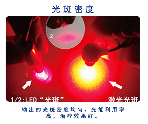
半导体激光治疗仪是骗局吗?

2016全球十大电子元器件分销商排行榜
2016年10大全球电子元器件代理商排行一览表
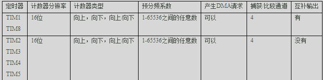
STM32学习笔记:通用定时器基本定时功能


 2012- 2022 拍明芯城ICZOOM.com 版权所有 客服热线:400-693-8369 (9:00-18:00)


