


 产品分类
产品分类
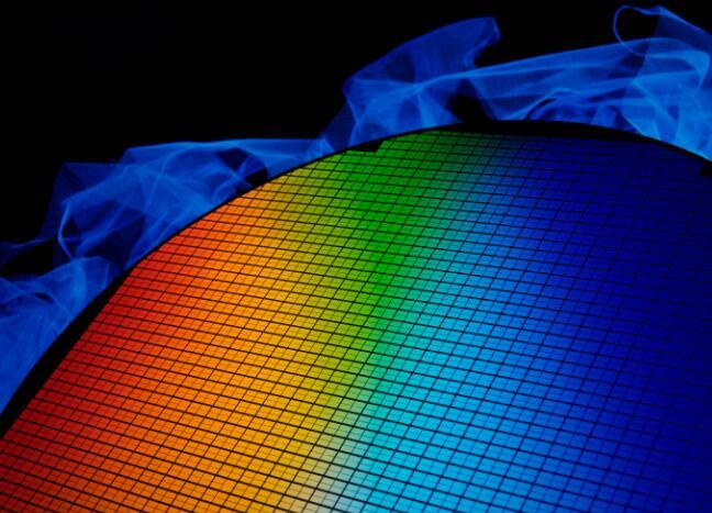
Heterogeneous integration and the evolution of IC packaging
 79
79
 拍明
拍明
原标题:Heterogeneous integration and the evolution of IC packaging
1. 核心概念解析
Heterogeneous Integration(异构集成)
指将不同工艺节点、材料或功能的芯片(如逻辑芯片、存储芯片、传感器、MEMS等)通过先进封装技术集成到一个系统中,实现性能、功耗和成本的优化。类比:将CPU(大脑)、GPU(图形处理)、DRAM(内存)等“模块”像拼积木一样组合,而非依赖单一芯片的“全能”设计。
IC Packaging Evolution(集成电路封装演变)
从传统引脚封装(如DIP)到2.5D/3D封装、Chiplet(小芯片)等,封装技术从“被动保护”转向“主动协同”,成为系统性能的关键瓶颈突破点。
2. 异构集成的驱动力
| 驱动力 | 具体表现 |
|---|---|
| 摩尔定律放缓 | 单芯片制程逼近物理极限(如3nm以下),异构集成通过架构创新延续性能提升。 |
| 应用需求多样化 | AI、5G、自动驾驶等需要同时满足高算力、低功耗、低延迟,单一芯片难以满足。 |
| 成本与良率 | 先进制程(如2nm)成本极高,异构集成可复用成熟制程芯片,降低整体成本。 |
| 供应链灵活性 | 不同厂商的芯片(如AMD CPU + 台积电CoWoS封装)可快速组合,缩短研发周期。 |

3. 关键封装技术演进
(1) 传统封装 → 先进封装
阶段1:引脚封装(如DIP、QFP)
功能:仅提供物理保护和电气连接。
缺点:I/O密度低、信号延迟高。
阶段2:BGA/CSP封装
优势:I/O密度提升10倍,适合移动设备。
案例:手机SoC的BGA封装。
(2) 2.5D/3D封装
2.5D封装(如CoWoS、EMIB)
原理:通过硅中介层(Interposer)连接多个芯片(如HBM堆叠内存+GPU)。
优势:带宽提升100倍,功耗降低50%。
案例:NVIDIA H100 GPU(CoWoS封装)。
3D封装(如TSV、混合键合)
原理:通过垂直通孔(TSV)或直接键合(如Cu-Cu键合)实现芯片堆叠。
优势:体积缩小50%,延迟降低至纳秒级。
案例:AMD 3D V-Cache(CPU+缓存堆叠)。
(3) Chiplet(小芯片)技术
原理:将大型SoC拆分为多个功能模块(如CPU核、I/O、AI加速器),通过封装级互连组合。
优势:
复用成熟IP,降低研发成本(如AMD Zen架构)。
灵活组合,支持定制化需求(如服务器芯片可扩展AI模块)。
标准:UCIe(Universal Chiplet Interconnect Express)联盟推动标准化。
4. 异构集成的挑战与解决方案
| 挑战 | 解决方案 |
|---|---|
| 热管理 | 3D堆叠导致局部热点,需采用液冷、微通道散热或动态功耗控制。 |
| 信号完整性 | 高速信号(如HBM3的8.4Gbps)需优化布线、引入重定时器(Retimer)。 |
| 测试与可靠性 | 封装后测试难度大,需开发预测试技术(如Known Good Die)和冗余设计。 |
| 供应链协同 | 需建立跨厂商协作机制(如Intel IDM 2.0模式)。 |
5. 未来趋势
Chiplet生态成熟
UCIe标准普及,推动跨厂商Chiplet组合(如AMD CPU + 第三方AI加速器)。
光互连替代电互连
硅光子技术(如Intel光I/O)解决电信号带宽瓶颈,支持100Tbps级传输。
封装即系统(System in Package, SiP)
将电源管理、射频、传感器等集成到单一封装,实现“即插即用”模块化设计。
AI驱动的封装设计
使用AI算法优化布线、热分布和信号完整性,缩短设计周期。
6. 行业案例
NVIDIA H100 GPU
采用台积电CoWoS-S封装,集成HBM3内存和GPU核心,带宽达3TB/s。
AMD MI300X APU
3D堆叠CPU+GPU+HBM3,实现1.5TB/s内存带宽,专为AI大模型设计。
苹果M1 Ultra
通过UltraFusion封装技术连接两片M1 Max,性能翻倍。
7. 总结
异构集成是后摩尔时代的必然选择:通过封装技术突破单芯片限制,实现性能、成本和灵活性的平衡。
封装技术从“配角”变“主角”:未来芯片性能的50%以上将由封装决定。
生态协作是关键:需跨厂商、跨学科(材料、热、信号)协同创新。
通过异构集成与先进封装,半导体行业正从“单一芯片竞争”转向“系统级竞争”,为AI、量子计算、6G等前沿技术提供底层支撑。
责任编辑:David
【免责声明】
1、本文内容、数据、图表等来源于网络引用或其他公开资料,版权归属原作者、原发表出处。若版权所有方对本文的引用持有异议,请联系拍明芯城(marketing@iczoom.com),本方将及时处理。
2、本文的引用仅供读者交流学习使用,不涉及商业目的。
3、本文内容仅代表作者观点,拍明芯城不对内容的准确性、可靠性或完整性提供明示或暗示的保证。读者阅读本文后做出的决定或行为,是基于自主意愿和独立判断做出的,请读者明确相关结果。
4、如需转载本方拥有版权的文章,请联系拍明芯城(marketing@iczoom.com)注明“转载原因”。未经允许私自转载拍明芯城将保留追究其法律责任的权利。
拍明芯城拥有对此声明的最终解释权。
相关资讯
:
云母电容公司_云母电容生产厂商
开关三极管13007的规格参数、引脚图、开关电源电路图?三极管13007可以用什么型号替代?
74ls74中文资料汇总(74ls74引脚图及功能_内部结构及应用电路)
芯片lm2596s开关电压调节器的中文资料_引脚图及功能_内部结构及原理图_电路图及封装
芯片UA741运算放大器的资料及参数_引脚图及功能_电路原理图?ua741运算放大器的替代型号有哪些?
28nm光刻机卡住“02专项”——对于督工部分观点的批判(睡前消息353期)


 2012- 2022 拍明芯城ICZOOM.com 版权所有 客服热线:400-693-8369 (9:00-18:00)


