基于NXP公司的S32K 32位汽车通用MCU开发方案
 369
369
 拍明
拍明
原标题:NXP S32K 32位汽车通用MCU开发方案
NXP公司的S32K是32位汽车通用MCU,工作电压2.7-5.5V,提供多种容量存储器,外设和封装选择.器件采用ARM™ Cortex-M4F/M0+核,支持高达112MHz,具有1.25Dhrystone MIPS/MHz性能,集成了数字信号处理器(DSP)以及可配置嵌套矢量中断控制器(NVIC)以及单精度浮点单元(FPU),主要用在汽车电子,物联(IoT)智能连接和马达控制.本文介绍了S32K主要特性,框图,评估板S32K144EVB主要特性,框图和电路图,
The S32K series further extends the highly scalable portfolio of ARM®Cortex®MCUs in the automotive industry. It builds on the legacy of theKEA series, whilst introducing higher memory options alongside a richerperipheral set extending capability into a variety of automotiveapplications.
With a 2.70–5.5 V supply and focus on automotive environmentrobustness, the S32K series devices are well suited to a wide range ofapplications in electrical harsh environments. These devices are optimizedfor cost-sensitive applications offering low pin-count options.
The S32K series offers a broad range of memory, peripherals, andpackage options. They share common peripherals and pin counts allowingdevelopers to migrate easily within the MCU family or among the MCUfamilies to take advantage of more memory or feature integration. Thisscalability allows developers to standardize on the S32K series for their
end product platforms, maximizing hardware and software reuse andreducing timeto-market.
S32K is a scalable family of AEC-Q100 qualified 32-bit ARM Cortex-M4F and Cortex-M0+ based MCUs targeted for general purpose automotive and high reliability industrial applications.
Scalability – hardware and software compatible families with multiple performance, memory and feature options Integration – ISO CAN FD, CSEc hardware security, ASIL-B ISO26262 functional safety, ultra-low power performance Software – free automotive-grade Software Development Kit (SDK) and S32 Design Studio IDE, AUTOSAR & MCAL support, third party ecosystem.
S32K主要特性:
• Operating characteristics
– Voltage range: 2.7 V to 5.5 V
– Ambient temperature range: -40 ℃ to 105 ℃ forHSRUN, -40 ℃ to 125 ℃ for RUN
• ARM™ Cortex-M4F/M0+ core, 32-bit CPU
– Supports up to 112 MHz frequency with 1.25Dhrystone MIPS per MHz
– ARM Core based on the ARMv7 Architecture andThumb?-2 ISA
– Integrated Digital Signal Processor (DSP)
– Configurable Nested Vectored Interrupt Controller(NVIC)
– Single Precision Floating Point Unit (FPU)
• Clock interfaces
– 4 - 40 MHz fast external oscillator (SOSC)
– 48 MHz Fast Internal RC oscillator (FIRC)
– 8 MHz Slow Internal RC oscillator (SIRC)
– 128 kHz Low Power Oscillator (LPO)
– Up to 112 MHz System Phased Lock Loop (SPLL)
– Up to 50 MHz DC external square wave input clock
– Real Time Counter (RTC)
• Power management
– Low-power ARM Cortex-M4F/M0+ core withexcellent energy efficiency
– Power Management Controller (PMC) with multiplepower modes: HSRUN, Run, Stop, VLPR, andVLPS
– Supports peripheral specific clock gating. Onlyspecific peripherals remain working in low powermodes.
• Memory and memory interfaces
– Up to 2 MB program flash memory with ECC
– 64 KB FlexNVM for data flash memory with ECCand EEPROM emulation
– Up to 256 KB SRAM with ECC
– Up to 4 KB of FlexRAM for use as SRAM orEEPROM emulation
– Up to 4 KB Code cache to minimize performanceimpact of memory access latencies
– QuadSPI with HyperBus™ support
• Mixed-signal analog
– Up to two 12-bit Analog-to-Digital Converter(ADC) with up to 32 channel analog inputs permodule
– One Analog Comparator (CMP) with internal 8-bitDigital to Analog Converter (DAC)
• Debug functionality
– Serial Wire JTAG Debug Port (SWJ-DP) combines
– Debug Watchpoint and Trace (DWT)
– Instrumentation Trace Macrocell (ITM)
– Test Port Interface Unit (TPIU)
– Flash Patch and Breakpoint (FPB) Unit
• Human-machine interface (HMI)
– Up to 156 GPIO pins with interrupt functionality
– Non-Maskable Interrupt (NMI)
• Communications interfaces
– Up to three Low Power Universal AsynchronousReceiver/Transmitter (LPUART) modules withDMA support and low power availability
– Up to three Low Power Serial Peripheral Interface(LPSPI) modules with DMA support and low poweravailability
– Up to two Low Power Inter-Integrated Circuit(LPI2C) modules with DMA support and low poweravailability
– Up to three FlexCAN modules (with optional CANFDsupport)
– FlexIO module for flexible and high performanceserial interfaces
• Reliability, safety and security
– HW Security Engine (CSEc)
– Internal watchdog (WDOG)
– External Watchdog monitor (EWM) module
– Error-Correcting Code (ECC) on flash and SRAMmemories
– Cyclic Redundancy Check (CRC) module
– 128-bit Unique Identification (ID) number
– System Memory Protection Unit (System MPU)
• Timing and control
– Up eight independent 16-bit FlexTimers (FTM) module, offering up to 64 standard channels (IC/OC/PWM)
– One 16-bit Low Power Timer (LPTMR) with flexible wake up control
– Two Programmable Delay Blocks (PDB) with flexible trigger system
– One 32-bit Low Power Interrupt Timer (LPIT) with 4 channels
– 32-bit Real Time Counter (RTC)
• I/O and package
– 32-pin QFN, 48-pin LQFP, 64-pin LQFP, 100-pin LQFP, MAPBGA-100, 144-pin LQFP, 176-pin LQFP packageoptions
• 16 channel DMA with up to 63 request sources using DMAMUX
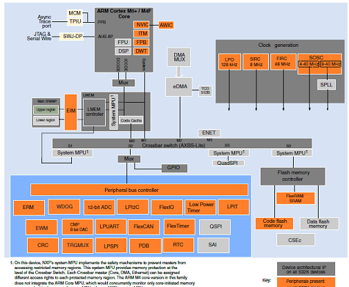
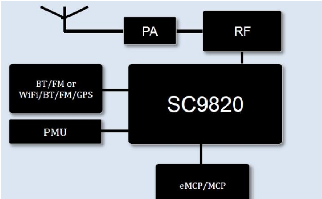
图1.S32K框图
S32K目标应用:
Automotive
Smart Connected Solutions for the Internet of Things (IoT)
Motor Control
评估板S32K144EVB
The S32K144EVB is low cost evaluation platform and development system for quick application prototyping and demonstration for the S32K144 MCU.

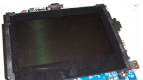
图2.评估板S32K144EVB外形图
评估板S32K144EVB主要特性:
•Supports S32K144 100LQFP
•Small form factor size supports up to 6” x 4”
•Arduino™ UNO footprint-compatible with expansion “shield” support
•Integrated open-standard serial and debug adapter (OpenSDA) with support for several industry-standard debug interfaces
•Easy access to the MCU I/O header pins for prototyping
•On-chip connectivity for CAN, LIN, UART/SCI.
•SBC UJA1169 and LIN phyTJA1027
•Potentiometer for precise voltage and analog measurement
•RGB LED
•Two push-button switches (SW2 and SW3) and two touch electrodes
•Flexible power supply options
•microUSBor
•external 12V power supply
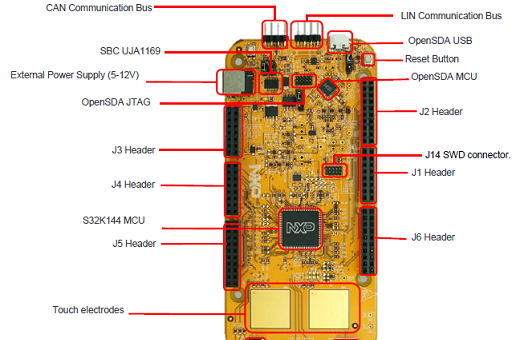
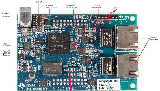
图3.评估板S32K144EVB主要元件分布图
详情请见:
责任编辑:HanFeng
【免责声明】
1、本文内容、数据、图表等来源于网络引用或其他公开资料,版权归属原作者、原发表出处。若版权所有方对本文的引用持有异议,请联系拍明芯城(marketing@iczoom.com),本方将及时处理。
2、本文的引用仅供读者交流学习使用,不涉及商业目的。
3、本文内容仅代表作者观点,拍明芯城不对内容的准确性、可靠性或完整性提供明示或暗示的保证。读者阅读本文后做出的决定或行为,是基于自主意愿和独立判断做出的,请读者明确相关结果。
4、如需转载本方拥有版权的文章,请联系拍明芯城(marketing@iczoom.com)注明“转载原因”。未经允许私自转载拍明芯城将保留追究其法律责任的权利。
拍明芯城拥有对此声明的最终解释权。


 产品分类
产品分类




 2012- 2022 拍明芯城ICZOOM.com 版权所有 客服热线:400-693-8369 (9:00-18:00)


