产品分类
产品分类
基于EFM8UB10F16G-C-QFN20R/EFM8BB31F64G-B-QFN32主控器件的Type-C视频转换器解决方案
 374
374
 拍明
拍明
Type-C全称USB Type-C接口,是一种全新的USB接口形式,它伴随最新的USB3.1标准横空出世。由USB-IF组织于2014年8月份发布,是USB标准化组织为了解决USB接口长期以来物理接口规范不统一,电能只能单向传输等弊端而制定的全新数据、视频、音频、电能传输接口规范。由于Type-C具有传输速度快、接口小巧、支持正反向插入等特点,Type-C取代视频接口将成为以后的发展趋势,而Type-C视频转换器将成为视频输出的必需品,本文接下来会介绍一款基于EFM8UB1+EFM8BB3的Type-C视频转换器整体解决方案。
【EFM8UB1】
元件供应
型号:EFM8UB10F16G-C-QFN20R 品牌:SILICON LABS
型号:EFM8UB10F8G-C-QFN20R 品牌:SILICON LABS
型号:EFM8UB10F16G-C-QFN28 品牌:SILICON LABS
UG240: EFM8UB1-SLSTK2000A User's Guide
The EFM8UB1-SLSTK2000A is an excellent starting point to get familiar with the EFM8 EFM8UB1 Universal Bee microcontrollers.
The kit contains sensors and peripherals demonstrating some of the MCU's many capabilities.
The kit can also serve as a starting point for application development.

The kit includes the following:
• EFM8UB1 Universal Bee Starter Kit Board
• 1 x CR2032 battery
• Getting Started card
• 1 x mini and 1 x micro USB cables
KEY FEATURES
• EFM8UB10F16G MCU with 16 KB Flash and 2 KB RAM.
• 20-pin expansion header.
• Power sources include USB and CR2032 battery.
• 2 user buttons, 1 tri-color LED.
• 8-direction joystick.
• Ultra low power 128x128 pixel MemoryLCD.
1. Getting Started
Hardware
To set up the hardware for the EFM8UB1-SLSTK2000A kit:
1. Provide power to the board by connecting the USB connector to the PC using the provided USB cable.
2. Move the switch to the Advanced Energy Monitor (AEM) position.

Figure 1.1. Hardware Setup
Software
The first step to get started with your new EFM8UB1-SLSTK2000A is to go to
The Simplicity Studio software package contains all the tools, drivers, software examples and documentation needed to use the
EFM8UB1 Starter Kit. The board comes pre-loaded with a default application, Space Invaders, to interact with while the software downloads.
After downloading the latest version of Simplicity Studio and installing:
1. Select the J-Link adapter for the kit under [Devices].
2. Click one of the demos available under [Getting Started]>[Demos] or click the [Getting Started]>[Demos]>[View All] to view the
entire list of available demos.
3. Click the [Rainbow Blinky] demo and click [Start] to download and run the demo.
Additional demos showcasing the various features of the EFM8 are also available in Simplicity Studio.
2. Kit Block Diagram
An overview of the EFM8UB1 Starter Kit is shown in the figure below.

Figure 2.1. EFM8UB1-SLSTK2000A Block Diagram
3. Kit Hardware Layout
The layout of the EFM8UB1 Starter Kit is shown below.

Figure 3.1. EFM8UB1-SLSTK2000A Hardware Layout
Figure 3.1. EFM8UB1-SLSTK2000A Hardware Layout
The EFM8 device on the kit is connected to several peripherals. The table below shows all of the external connections to the MCU.
Table 3.1. Kit MCU Connections


【EFM8BB3】
元件供应
型号:EFM8BB31F64G-B-QFN32 品牌:SILICON LABS
型号:EFM8BB31F64G-B-QFN24R 品牌:SILICON LABS
型号:EFM8BB31F64G-B-QFP32 品牌:SILICON LABS
EFM8 Busy Bee Family EFM8BB3 Reference Manual
The EFM8BB3, part of the Busy Bee family of MCUs, is a performance line of 8-bit microcontrollers with a comprehensive analog and digital feature set in small packages.
These devices offer state-of-the-art performance by integrating 12-bit ADC, internal temperature sensor, and up to four 12-bit DACs into small packages, making them ideal for general purpose applications. With an efficient, pipelined 8051 core with maximum operating frequency at 50 MHz, various communication interfaces, and four channels of configurable logic, the EFM8BB3 family is optimal for many embedded applications.
EFM8BB3 applications include the following:
• Consumer electronics
• Precision instrumentation
• Power management and control
• Industrial control and automation
• Smart sensors
• Automotive control
KEY FEATURES
• Pipelined 8-bit 8051 MCU Core with 50 MHz operating frequency
• Up to 29 multifunction I/O pins
• One 12-bit/10-bit ADC
• Four 12-bit DACs with synchronization and PWM capabilities
• Two low-current analog comparators with built-in reference DACs
• Internal temperature sensor
• Internal 49 MHz and 24.5 MHz oscillators accurate to ±2%
• Four channels of Configurable Logic
• 6-channel PWM / PCA
• Six 16-bit general-purpose timers


Figure 1.1. Detailed EFM8BB3 Block Diagram
This section describes the EFM8BB3 family at a high level. For more information on each module including register definitions, see the EFM8BB3 Reference Manual.
Power
All internal circuitry draws power from the VDD supply pin. External I/O pins are powered from the VIO supply voltage (or VDD on devices without a separate VIO connection), while most of the internal circuitry is supplied by an on-chip LDO regulator. Control over the device power can be achieved by enabling/disabling individual peripherals as needed. Each analog peripheral can be disabled when not in use and placed in low power mode. Digital peripherals, such as timers and serial buses, have their clocks gated off and draw little power when they are not in use.
Table 1.1. Power Modes
I/O
Digital and analog resources are externally available on the device’s multi-purpose I/O pins. Port pins P0.0-P2.3 can be defined as general-purpose
I/O (GPIO), assigned to one of the internal digital resources through the crossbar or dedicated channels, or assigned to an
analog function. Port pins P2.4 to P3.7 can be used as GPIO. Additionally, the C2 Interface Data signal (C2D) is shared with P3.0 or
P3.7, depending on the package option.
The port control block offers the following features:
• Up to 29 multi-functions I/O pins, supporting digital and analog functions.
• Flexible priority crossbar decoder for digital peripheral assignment.
• Two drive strength settings for each port.
• State retention feature allows pins to retain configuration through most reset sources.
• Two direct-pin interrupt sources with dedicated interrupt vectors (INT0 and INT1).
• Up to 24 direct-pin interrupt sources with shared interrupt vector (Port Match).
EFM8BB3 Reference Manual
System Overview
silabs.com | Building a more connected world. Rev. 0.4 | 14
1.4 Clocking
The CPU core and peripheral subsystem may be clocked by both internal and external oscillator resources. By default, the system clock comes up running from the 24.5 MHz oscillator divided by 8.
The clock control system offers the following features:
• Provides clock to core and peripherals.
• 24.5 MHz internal oscillator (HFOSC0), accurate to ±2% over supply and temperature corners.
• 49 MHz internal oscillator (HFOSC1), accurate to ±2% over supply and temperature corners.
• 80 kHz low-frequency oscillator (LFOSC0).
• External RC, CMOS, and high-frequency crystal clock options (EXTCLK).
• Clock divider with eight settings for flexible clock scaling:
• Divide the selected clock source by 1, 2, 4, 8, 16, 32, 64, or 128.
• HFOSC0 and HFOSC1 include 1.5x pre-scalers for further flexibility.
1.5 Counters/Timers and PWM Programmable Counter Array (PCA0) The programmable counter array (PCA) provides multiple channels of enhanced timer and PWM functionality while requiring less CPU intervention than standard counter/timers. The PCA consists of a dedicated 16-bit counter/timer and one 16-bit capture/compare module for each channel. The counter/timer is driven by a programmable timebase that has flexible external and internal clocking options.
Each capture/compare module may be configured to operate independently in one of five modes: Edge-Triggered Capture, Software Timer, High-Speed Output, Frequency Output, or Pulse-Width Modulated (PWM) Output. Each capture/compare module has its own associated I/O line (CEXn) which is routed through the crossbar to port I/O when enabled.
• 16-bit time base
• Programmable clock divisor and clock source selection
• Up to six independently-configurable channels
• 8, 9, 10, 11 and 16-bit PWM modes (center or edge-aligned operation)
• Output polarity control
• Frequency output mode
• Capture on rising, falling or any edge
• Compare function for arbitrary waveform generation
• Software timer (internal compare) mode
• Can accept hardware “kill” signal from comparator 0 or comparator 1
Timers (Timer 0, Timer 1, Timer 2, Timer 3, Timer 4, and Timer 5) Several counter/timers are included in the device: two are 16-bit counter/timers compatible with those found in the standard 8051, and the rest are 16-bit auto-reload timers for timing peripherals or for general purpose use. These timers can be used to measure time intervals, count external events and generate periodic interrupt requests. Timer 0 and Timer 1 are nearly identical and have four primary modes of operation. The other timers offer both 16-bit and split 8-bit timer functionality with auto-reload and capture capabilities.
Timer 0 and Timer 1 include the following features:
• Standard 8051 timers, supporting backwards-compatibility with firmware and hardware.
• Clock sources include SYSCLK, SYSCLK divided by 12, 4, or 48, the External Clock divided by 8, or an external pin.
• 8-bit auto-reload counter/timer mode
• 13-bit counter/timer mode
• 16-bit counter/timer mode
• Dual 8-bit counter/timer mode (Timer 0)
Timer 2, Timer 3, Timer 4, and Timer 5 are 16-bit timers including the following features:
• Clock sources for all timers include SYSCLK, SYSCLK divided by 12, or the External Clock divided by 8
• LFOSC0 divided by 8 may be used to clock Timer 3 and Timer 4 in active or suspend/snooze power modes
• Timer 4 is a low-power wake source, and can be chained together with Timer 3
• 16-bit auto-reload timer mode
• Dual 8-bit auto-reload timer mode
• External pin capture
• LFOSC0 capture
• Comparator 0 capture
• Configurable Logic output capture
Watchdog Timer (WDT0)
The device includes a programmable watchdog timer (WDT) running off the low-frequency oscillator. A WDT overflow forces the MCU into the reset state. To prevent the reset, the WDT must be restarted by application software before overflow. If the system experiences a software or hardware malfunction preventing the software from restarting the WDT, the WDT overflows and causes a reset. Following a reset, the WDT is automatically enabled and running with the default maximum time interval. If needed, the WDT can be disabled by system software or locked on to prevent accidental disabling. Once locked, the WDT cannot be disabled until the next system reset.
The state of the RST pin is unaffected by this reset.
The Watchdog Timer has the following features:
• Programmable timeout interval
• Runs from the low-frequency oscillator
• Lock-out feature to prevent any modification until a system reset
1.6 Communications and Other Digital Peripherals Universal Asynchronous Receiver/Transmitter (UART0) UART0 is an asynchronous, full duplex serial port offering modes 1 and 3 of the standard 8051 UART. Enhanced baud rate support allows a wide range of clock sources to generate standard baud rates. Received data buffering allows UART0 to start reception of asecond incoming data byte before software has finished reading the previous data byte.
The UART module provides the following features:
• Asynchronous transmissions and receptions.
• Baud rates up to SYSCLK/2 (transmit) or SYSCLK/8 (receive).
• 8- or 9-bit data.
• Automatic start and stop generation.
• Single-byte FIFO on transmit and receive.
Type-C视频转换器整体解决方案。
随着Type-C的发布,视频电子标准协会(Video Electronics Standards Association, VESA)也针对Type-C发布了DisplayPort Alternate Mode on USB Type-C接口标准,即DP交替模式,该标准允许通过一根USB Type-C数据线达成DisplayPort信号传输及供电。DP交替模式的进入,需要通过一定的协议,这部分协议可以通过8位单片机EFM8UB1及EFM8BB3实现。下图是基于EFM8UB1+EFM8BB3的Type-C视频转换器方案框图:
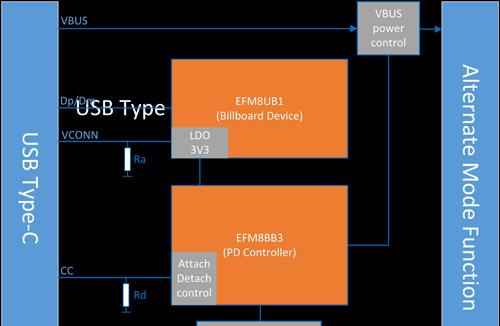
图1: Type-C视频转换器方案框图
该框图分2个部分:Billboard设备及PD控制器,Billboard设备由EFM8UB1实现。EFM8UB1是基于8051内核的MCU,带有全速USB2.0接口、具有多通道高速串行外设,支持充电器检测协议(USB BCS V1.2)。基于EFM8UB1的Billboard设备,支持USB主机通信,向其提供设备信息,并支持信息弹窗。
PD控制器用于CC逻辑控制,由EFM8BB3实现。EFM8BB3同样基于C0851内核,内置PD协议,主频高达50MHZ。内部的12位ADC,用于监控CC逻辑信号、插拔检测及正反面检测。该MCU具有CLU逻辑控制单元,可快速实现BMC数据的发送及接收。在PD控制器中,EFM8BB3可实现电源控制协议(UFP&DFP)、交替模式检测及控制。
【Type-C接口】
2013年12月,USB 3.0推广团队已经公布了下一代 USB Type-C 连接器的渲染图,随后在2014年8月开始已经准备好进行大规模量产。新版接口的亮点在于更加纤薄的设计、更快的传输速度(最高10Gbps)以及更强悍的电力传输(最高100W)。Type-C双面可插接口最大的特点是支持USB接口双面插入,正式解决了“USB永远插不准”的世界性难题,正反面随便插。同时与它配套使用的USB数据线也必须更细和更轻便。 2015年8月1日,特科芯推出了全球首款Type-C接口的移动固态硬盘。2016年1月1日,特科芯推出了全球首款Type-C接口的指纹加密移动固态硬盘。
诺基亚N1在正式公布的时候,官方曾经表示该产品将支持最新的 Type-C USB接口,不过当时并没有引起外界足够的重视。不过看来诺基亚对N1的这个特性寄予了厚望,因此再一次在官方Twitter账户上又一次强调了这个特性。
诺基亚在Twitter上写道:“诺基亚N1使用双面可插的Type-C接口,这将极大地方便用户使用”。
多数人可能并不知道Type-C双面可插接口是什么样子,但业内人士相信,这个功能一旦在移动设备上普及开来,一定会受到大家的欢迎。
2015年3月9日,在美国举行的苹果新品发布会上,全新MacBook首次在笔记本电脑上将电源接口、USB接口、DP接口、HDMI接口与VGA接口统一用一个USB-C来承载,这是USB-C技术第一次在消费级笔记本电脑的应用。随着Type-C连接器的到来,数据传输将更加便利。USB-C最大的特点是正反都可以插入!
2015年8月1日,特科芯推出了全球首款Type-C接口的移动固态硬盘。该款SSD提供了最新的Type-C接口,支持USB接口双面插入。特科芯移动固态硬盘也分为旗舰级和标准级两款产品,旗舰级无疑是速度更快可靠度更高,偏向商务或者发烧型用户。而标准级产品则面向主流大众用户,但实际传输速度也快的惊人。
【视频转换器】
视频转换器涵盖了各种视频格式的转换工具,比如:3GP视频格式转换器,AVI转换器,MP4转换工具,FLV转换软件等视频转换工具。他们不仅有易于操作的界面,而且支持批量转换处理,将各种视频快速转换为流行的媒体文件格式。
1、Microsoft RLE
一种8位的编码方式,只能支持到256色。压缩动画或者是计算机合成的图像等具有大面积色块的素材可以使用它来编码,是一种无损压缩方案。
2、Microsoft Video 1
是微软早期开发的一种压缩器,是一种有损压缩方案,最高仅达到256色,由于颜色少,所以品质很低,但在需要大分辨率同时又要求体积超小的特殊情况下,就非常有用,比如远程桌面传输等用途。
3、Microsoft H.261和H.263 Video Codec
用于视频会议的Codec,其中H.261适用于ISDN、DDN线路,H.263适用于局域网,不过一般机器上这种Codec是用来播放的,不能用于编码。
4、Intel Indeo Video R3.2
所有的Windows版本都能用Indeo video 3.2播放AVI编码。它压缩率比Cinepak大,但需要回放的计算机要比Cinepak的快。
5、Intel Indeo Video 4和5
常见的有4.5和5.10两种,质量比Cinepak和R3.2要好,可以适应不同带宽的网络,但必须有相应的解码插件才能顺利地将下载作品进行播放。适合于装了Intel公司MMX以上CPU的机器,回放效果优秀。如果一定要用AVI的话,推荐使用5.10,在效果几乎一样的情况下,它有更快的编码速度和更高的压缩比。
6、Intel IYUV Codec
使用该方法所得图像质量极好,因为此方式是将普通的RGB色彩模式变为更加紧凑的YUV色彩模式。如果你想将AVI压缩成MPEG-1的话,用它得到的效果比较理想,只是它的生成的文件太大了
7、Microsoft MPEG-4 Video codec
常见的有1.0、2.0、3.0三种版本,当然是基于MPEG-4技术的,其中3.0并不能用于AVI的编码,只能用于生成支持“视频流”技术的ASF文件。
8、DivX- MPEG-4 Low-Motion/Fast-Motion
实际与Microsoft MPEG-4 Video code是相当的东西,只是Low-Motion采用的固定码率,Fast-Motion采用的是动态码率,后者压缩成的AVI几乎只是前者的一半大,但质量要差一些。Low-Motion适用于转换DVD以保证较好的画质,Fast-Motion用于转换VCD以体现MPEG-4短小精悍的优势。
9 、DivX
实际上就是DivX,是目前最为流行和出色的编码器之一。原来DivX是为了打破Microsoft的ASF规格而开发的,开发组摇身一变成了Divxnetworks公司,不断推出新的版本,成就了今天的地位。DivX最大的特点是它对硬件进行了彻底的优化,编码效率非常高,此外,它的画面质量也非常优秀,最大限度地让编码速度和画面质量完美兼得。在编码程序中还支持1-pass和2-pass的设置,2-pass相当于两次编码,这样可以最大限度地在画面质量与文件体积中取得最大的平衡,也就是以较小的体积获得较高的质量,方便网络共享。
责任编辑:Davia
【免责声明】
1、本文内容、数据、图表等来源于网络引用或其他公开资料,版权归属原作者、原发表出处。若版权所有方对本文的引用持有异议,请联系拍明芯城(marketing@iczoom.com),本方将及时处理。
2、本文的引用仅供读者交流学习使用,不涉及商业目的。
3、本文内容仅代表作者观点,拍明芯城不对内容的准确性、可靠性或完整性提供明示或暗示的保证。读者阅读本文后做出的决定或行为,是基于自主意愿和独立判断做出的,请读者明确相关结果。
4、如需转载本方拥有版权的文章,请联系拍明芯城(marketing@iczoom.com)注明“转载原因”。未经允许私自转载拍明芯城将保留追究其法律责任的权利。
拍明芯城拥有对此声明的最终解释权。
相关资讯
:
基于MC33771主控芯片的新能源锂电池管理系统解决方案

AMIC110 32位Sitara ARM MCU开发方案

基于AMIC110多协议可编程工业通信处理器的32位Sitara ARM MCU开发方案

基于展讯SC9820超低成本LTE芯片平台的儿童智能手表解决方案

基于TI公司的AM437x双照相机参考设计

基于MTK6580芯片的W2智能手表解决方案


 2012- 2022 拍明芯城ICZOOM.com 版权所有 客服热线:400-693-8369 (9:00-18:00)