基于EFM8UB20/ISL3177E主控器件的基站授时系统解决方案
 270
270
 拍明
拍明
概述
基站里不同的设备都有RS485对外接口,通讯接口有20Mbps和40Mbps两种不同速度,为了使各设备实现同步需要MCU从GNSS获取时钟,再通过RS485总线统一各设备时间一致性,同时把信息保存下来。为实现上述功能需要双串口高速的MCU以及带ESD保护功能的全双工RS485芯片。
优势
· Silicon Labs 8位MCU EFM8UB20,系统时钟速度可达48MHz,内部系统时钟精度±1.5%,内置64K Flash、4K XRAM,丰富的外设资源(两个UART、一个IIC、一个SPI、40个GPIO口),TQPF48封装满足产品设计需求,-40℃到85℃工业级工作范围,两种供电方式可选,包括2.65V到 3.6 V供电或使用内部集成5V转3.3V LDO 5V供电。主推型号,性价比高。
【EFM8UB20】
EFM8UB属于Universal Bee系列MCU,为业界集成度最高、带USB接口的混合信号8位微控制器。EFM8UB2搭载高精度振荡器、时钟恢复电路以及集成收发器,不需要任何外部元件即可用于所有全速USB应用。
产品特色
流水线式8位8051 MCU内核,最大工作频率达48 MHz
兼容无晶振全速/低速USB 2.0的控制器,具有1kB缓冲区
一个单端差分10位ADC和两个模拟比较器
内部48MHz振荡器支持无晶振USB和UART操作,在使用USB时钟恢复时精度为±0.25%
2个UART、1个SPI、2个SMBus/I2C串行通信接口
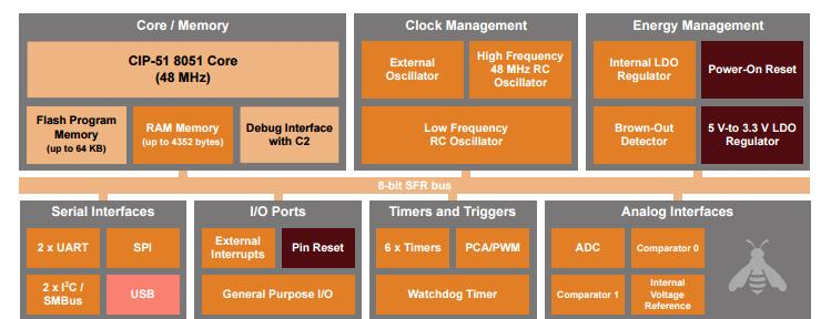
EFM8UB20框图
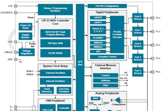
EFM8 Universal Bee Family EFM8UB2 Data Sheet
The EFM8UB2, part of the Universal Bee family of MCUs, is a multi-purpose line of 8-bit microcontrollers with USB feature set.
These devices offer high value by integrating a USB peripheral interface with a high precision oscillator, clock recovery circuit, and integrated transceiver, making them ideal for any full speed USB applications with no external components required. With an efficient 8051 core and precision analog, the EFM8UB2 family is also optimal for embedded applications.
EFM8UB2 applications include the following:
• USB I/O controls, dongles
• High-speed communication bridge
• Consumer electronics
• Medical equipment
KEY FEATURES
• Pipelined 8-bit 8051 MCU Core with 48 MHz maximum operating frequency
• Up to 40 multifunction I/O pins
• Crystal-less full speed/low speed USB 2.0 compliant controller with 1 KB buffer memory
• One differential 10-bit ADC and two analog comparators
• Internal 48 MHz oscillator with ±0.25% accuracy with USB clock recovery supports crystal-free USB and UART operation
• 2 UARTs, SPI, 2 SMBus/I2C serial communications
Feature List
The EFM8UB2 highlighted features are listed below.
• Core:
• Pipelined CIP-51 Core
• Fully compatible with standard 8051 instruction set
• 70% of instructions execute in 1-2 clock cycles
• 48 MHz maximum operating frequency
• Memory:
• Up to 64 KB flash memory, in-system re-programmable from firmware.
• Up to 4352 bytes RAM (including 256 bytes standard 8051 RAM and 4096 bytes on-chip XRAM)
• Power:
• Internal LDO regulator for CPU core voltage
• Internal 5-to-3.3 V LDO allows direct connection to USB supply net
• Power-on reset circuit and brownout detectors
• I/O: Up to 40 total multifunction I/O pins:
• Flexible peripheral crossbar for peripheral routing
• 10 mA source, 25 mA sink allows direct drive of LEDs
• Clock Sources:
• Internal 48 MHz precision oscillator ( ±1.5% accuracy without USB clock recovery, ±0.25% accuracy with USB clock recovery)
• Internal 80 kHz low-frequency oscillator
• External crystal, RC, C, and CMOS clock options
• Timers/Counters and PWM:
• 5-channel Programmable Counter Array (PCA) supporting PWM, capture/compare, and frequency output modes with watchdog timer function
• 6 x 16-bit general-purpose timers
• Communications and Digital Peripherals:
• Universal Serial Bus (USB) Function Controller with eight
flexible endpoint pipes, integrated transceiver, and 1 KB
FIFO RAM
• 2 x UART
• SPI™ Master / Slave
• 2 x SMBus™/I2C™ Master / Slave
• External Memory Interface (EMIF)
• Analog:
• 10-Bit Analog-to-Digital Converter (ADC0)
• 2 x Low-current analog comparators
• On-Chip, Non-Intrusive Debugging
• Full memory and register inspection
• Four hardware breakpoints, single-stepping
• Pre-loaded USB bootloader
• Temperature range -40 to 85 ºC
• Single power supply 2.65 to 3.6 V
• QFP48, QFP32, and QFN32 packages
With on-chip power-on reset, voltage supply monitor, watchdog timer, and clock oscillator, the EFM8UB2 devices are truly standalone system-on-a-chip solutions. The flash memory is reprogrammable in-circuit, providing non-volatile data storage and allowing field upgrades of the firmware. The on-chip debugging interface (C2) allows non-intrusive (uses no on-chip resources), full speed, in-circuit debugging using the production MCU installed in the final application. This debug logic supports inspection and modification of memory and registers, setting breakpoints, single stepping, and run and halt commands. All analog and digital peripherals are fully functional while debugging. Each device is specified for 2.65 to 3.6 V operation and is available in 32-pin QFN, 32-pin QFP, or 48-pin QFP packages. All package options are lead-free and RoHS compliant.
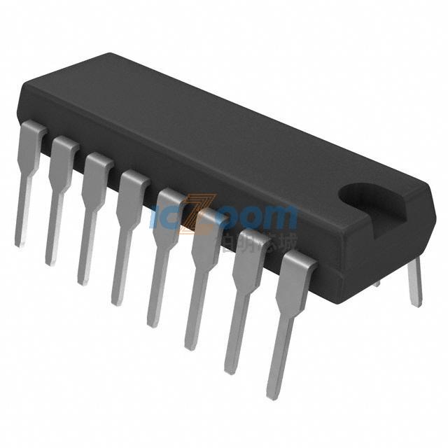
· Intersil的RS485通讯芯片ISL3177E,供电范围3V到3.6V,总线上可接入256个设备,-40℃到85℃工业级工作范围,MSOP8和SOIC两种封装可供选用,支持热插拔。20Mbps全双工通讯,±15kV IEC61000标准 ESD 保护使通讯安全可靠。
【ISL3177E】
±15kV IEC ESD Protected, 3.3V, Full-duplex, 20Mbps RS-485/RS-422 Transceiver
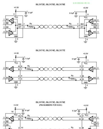
Key Features
IEC61000 ESD protection on RS-485 I/O pins: ±15kV
Class 3 ESD Level on all other pins: >7kV HBM
Full fail-safe (open, short, terminated/floating) receivers
Hot plug - Tx and Rx outputs remain three-state during power-up (only versions with output enable pins)
True 1/8 unit load allows up to 256 devices on the bus
Single 3.3V supply
High data rates: up to 20Mbps
Low quiescent supply current: 800μA (Max)
Ultra low shutdown supply current: 10nA
-7V to +12V common mode input/output voltage range
Half and full duplex pinouts
Three state Rx and Tx outputs available
Current limiting and thermal shutdown for driver overload protection
Tiny MSOP packages consume 50% less board space
Pb-free (RoHS compliant)
Description
The Intersil ISL317xE are ±15kV IEC61000 ESD protected, 3.3V powered single transceivers that meet both the RS-485 and RS-422 standards for balanced communication. These devices have very low bus currents (+125mA/-100mA), so they present a true “1/8 unit load” to the RS-485 bus. This allows up to 256 transceivers on the network without violating the RS-485 specification’s 32 unit load maximum, and without using repeaters. For example, in a remote utility meter reading system, individual meter readings are routed to a concentrator using an RS-485 network, so the high allowed node count minimizes the number of repeaters required.
Receiver (Rx) inputs feature a “Full Fail-Safe” design, which ensures a logic high Rx output if Rx inputs are floating, shorted, or terminated but undriven.
Hot Plug circuitry ensures that the Tx and Rx outputs remain in a high impedance state while the power supply stabilizes.
The ISL3170E through ISL3175E utilize slew rate limited drivers which reduce EMI, and minimize reflections from improperly terminated transmission lines, or unterminated stubs in multidrop and multipoint applications. Slew rate limited versions also include receiver input filtering to enhance noise immunity in the presence of slow input signals.
The ISL3170E, ISL3171E, ISL3173E, ISL3174E, ISL3176E, ISL3177E are configured for full duplex (separate Rx input and Tx output pins) applications. The half duplex versions multiplex the Rx inputs and Tx outputs to allow transceivers with output disable functions in 8 Ld packages.
Applications
Automated utility meter reading systems
High node count systems
Field bus networks
Security camera networks
Building environmental control/lighting systems
Industrial/process control networks
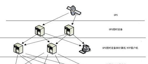
【授时系统】
授时系统 通过我国原子时系统AT(CSAO)和协调世界时UTC(CSAO)得到精密的时钟信号。为科研, 航天,航空,航海战略武器发射,民用各行业生产生活等各个领域,提供标准可靠的时钟信号。
中国的现代授时开启于1902年,中国海关曾制定海岸时,以东经120度之时刻为标准。位于北京的中央观象台将全国分为五个时区,1939年3月9日中华民国内政部召集标准时间会议,确认1912年划分之时区为中华民国标准时区。
1966年经国家科委批准筹建,1970年经周恩来总理批准短波授时台试播,1981年经国务院批准正式发播标准时间和频率信号;七十年代初,为适应中国战略武器发射、测控和空间技术发展的需要,经国务院和中央军委批准,在陕西天文台增建长波授时台(BPL),1986年通过由国家科委组织的国家级技术鉴定后正式发播标准时间、标准频率信号。
责任编辑:Davia
【免责声明】
1、本文内容、数据、图表等来源于网络引用或其他公开资料,版权归属原作者、原发表出处。若版权所有方对本文的引用持有异议,请联系拍明芯城(marketing@iczoom.com),本方将及时处理。
2、本文的引用仅供读者交流学习使用,不涉及商业目的。
3、本文内容仅代表作者观点,拍明芯城不对内容的准确性、可靠性或完整性提供明示或暗示的保证。读者阅读本文后做出的决定或行为,是基于自主意愿和独立判断做出的,请读者明确相关结果。
4、如需转载本方拥有版权的文章,请联系拍明芯城(marketing@iczoom.com)注明“转载原因”。未经允许私自转载拍明芯城将保留追究其法律责任的权利。
拍明芯城拥有对此声明的最终解释权。


 产品分类
产品分类



 2012- 2022 拍明芯城ICZOOM.com 版权所有 客服热线:400-693-8369 (9:00-18:00)


