TI SN75LVDS83B LCD屏FlatLink连接方案
 200
200
 拍明
拍明
原标题:TI SN75LVDS83B LCD屏FlatLink连接方案
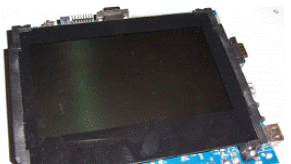
TI 公司的SN75lvds83B是FlatLink发送器,包括有四个7位并行负载串行输出的移为寄存器,7X时钟合成器,以及5个LVDS线路驱动器,可以把28位单端LVTTL数据同步地在5个平衡对导体上发送,由兼任的接收器接收如SN75LVDS82和集成了LVDS接收器的LCD屏.数据传输速率高达135M像素/秒,像素时肿范围从10MHz到135MHz,工作电压3.3V,75MHz时的功耗为170mW,可用于LCD屏驱动器,UMPC和笔记本电脑以及数码相框等.本文介绍了SN75LVDS83B的主要特性,方框图以及多种连接到LCD屏的应用电路和SN75LVDS83B评估模块电路图.
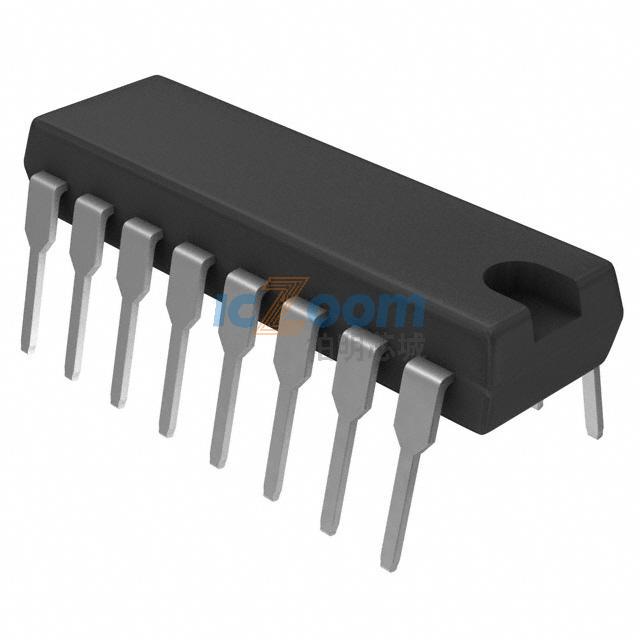
The SN75LVDS83B FlatLink™ transmitter contains four 7-bit parallel-load serial-out shift registers, a 7X clock synthesizer, and five Low-Voltage Differential Signaling (LVDS) line drivers in a single integrated circuit. These functions allow 28 bits of single-ended LVTTL data to be synchronously transmitted over five balanced-pair conductors for receipt by a compatible receiver, such as the SN75LVDS82 and LCD panels with integrated LVDS receiver.
When transmitting, data bits D0 through D27 are each loaded into registers upon the edge of the input clock signal (CLKIN). The rising or falling edge of the clock can be selected via the clock select (CLKSEL) pin. The frequency of CLKIN is multiplied seven times, and then used to unload the data registers in 7-bit slices and serially. The four serial streams and a phase-locked clock (CLKOUT) are then output to LVDS output drivers. The frequency of CLKOUT is the same as the input clock, CLKIN.
The SN75LVDS83B requires no external components and little or no control. The data bus appears the same at the input to the transmitter and output of the receiver with the data transmission transparent to the user(s). The only user intervention is selecting a clock rising edge by inputting a high level to CLKSEL or a falling edge with a low-level input, and the possible use of the Shutdown/Clear (SHTDN). SHTDN is an active-low input to inhibit the clock, and shut off the LVDS output drivers for lower power consumption. A low-level on this signal clears all internal registers to a low-level.
The SN75LVDS83B is characterized for operation over ambient air temperatures of -10℃ to 70℃.

SN75LVDS83B主要特性:
LVDS Display Serdes Interfaces Directly to LCD Display Panels with Integrated LVDS
Package Options: 4.5mm x 7mm BGA, and 8.1mm x 14mm TSSOP
1.8V up to 3.3V Tolerant Data Inputs to Connect Directly to Low-Power, Low-Voltage Application and Graphic Processors
Transfer Rate up to 135Mpps (Mega Pixel Per Second); Pixel Clock Frequency Range 10MHz to 135MHz
Suited for Display Resolutions Ranging From HVGA up to HD With Low EMI
Operates From a Single 3.3V Supply and 170mW (typ.) at 75MHz
28 Data Channels Plus Clock In Low-Voltage TTL to 4 Data Channels Plus Clock Out Low-Voltage Differential
Consumes Less Than 1mW When Disabled
Selectable Rising or Falling Clock Edge Triggered Inputs
ESD: 5kV HBM
Support Spread Spectrum Clocking (SSC)
Compatible with all OMAP™2x, OMAP™3x, and DaVinci™ Application Processors
SN75LVDS83B应用:
LCD Display Panel Driver
UMPC and Netbook PC
Digital Picture Frame

图1.SN75LVDS83B功能方框图

图2.SN75LVDS83B在24位彩色主机连接到24位LCD屏的应用

图3.SN75LVDS83B在18位彩色主机连接到18位LCD屏的应用

图4.SN75LVDS83B在12位彩色主机连接到18位LCD屏的应用

图5.SN75LVDS83B在24位彩色主机连接到18位LCD屏的应用

图6.SN75LVDS83B评估模块电路图
责任编辑:David
【免责声明】
1、本文内容、数据、图表等来源于网络引用或其他公开资料,版权归属原作者、原发表出处。若版权所有方对本文的引用持有异议,请联系拍明芯城(marketing@iczoom.com),本方将及时处理。
2、本文的引用仅供读者交流学习使用,不涉及商业目的。
3、本文内容仅代表作者观点,拍明芯城不对内容的准确性、可靠性或完整性提供明示或暗示的保证。读者阅读本文后做出的决定或行为,是基于自主意愿和独立判断做出的,请读者明确相关结果。
4、如需转载本方拥有版权的文章,请联系拍明芯城(marketing@iczoom.com)注明“转载原因”。未经允许私自转载拍明芯城将保留追究其法律责任的权利。
拍明芯城拥有对此声明的最终解释权。


 产品分类
产品分类



 2012- 2022 拍明芯城ICZOOM.com 版权所有 客服热线:400-693-8369 (9:00-18:00)


