产品分类
产品分类
ADI ADP1071-1/Couplers®隔离功能反激控制器解决方案
 108
108
 拍明
拍明
原标题:ADI ADP1071-1/Couplers®隔离功能反激控制器解决方案
ADI公司的ADP1071-1/ADP1071-2是集成了隔离功能和SR驱动器及轻负载模式的反激式控制器,消除了变压器和光耦合器件,降低了系统设计复杂性,成本和元件数量,并提高了系统可靠性.器件集成了误差放大器和优于1%精度基准电压,可编程开关频率50 kHz - 600 kHz,主要用在隔离的DC/DC和AC/DC转换器,通信和工业,小型基站,PoE供电设备,企业交换器和路由器.本文介绍了ADP1071-1 /ADP1071-2主要特性,框图,应用电路图以及评估板ADP1071-1EVALZ和评估板ADP1071-2EBZ3.3V主要特性,电路图,材料清单和PCB设计图.
The ADP1071-1/ADP1071-2 are pulse-width modulation (PWM) current mode fixed frequency synchronous flyback controllers designed for isolated dc-to-dc power supplies. Analog Devices proprietary iCouplers® are integrated in the ADP1071-1/ADP1071-2 to eliminate the bulky signal trans-formers and optocouplers that transmit signals over the isolation boundary. Integrating the iCouplers reduces system design complexity, cost, and component count and improves overall system reliability. With the integrated isolators and metal-oxide semiconductor field effect transistor (MOSFET) drivers on both the primary and the secondary side, the ADP1071-1/ADP1071-2 offer a compact system level design and yield a higher efficiency than a diode rectified flyback converter at heavy loads.
Output regulation is achieved by sensing the output voltage on the secondary side, where the feedback and the PWM signals are transmitted between the primary and secondary sides through the iCouplers.
The ADP1071-1/ADP1071-2 are offered in a 16-lead SOIC_W package with an isolation voltage rating of 5 kV rms. The ADP1071-2 is designed for isolated dc-to-dc applications typically with an input voltage less than 36 V, and the ADP1071-1 targets high input voltage applications, in which the dc input voltage can exceed 60 V.
The ADP1071-1/ADP1071-2 offer features such as input current protection, output overvoltage protection (OVP), undervoltage lockout (UVLO), precision enable with adjustable hysteresis, overtemperature protection (OTP), and power saving light load mode (LLM).
ADP1071-1/ADP1071-2主要特性:
Current mode controller for flyback topology
ADP1071-1: programmable LLM or CCM for high VIN applications
ADP1071-2: forced CCM operation
Programmable slope compensation
Integrated 5 kV isolation with Analog Devices, Inc., iCoupler technology
Wide voltage supply range
Primary VDD: up to 60 V (ADP1071-2 only)
Secondary VDD2: up to 36 V
Integrated 1 A primary side MOSFET driver
Integrated 1 A secondary side MOSFET drivers for synchronous rectification
Integrated error amplifier and <1% accurate reference voltage
Programmable frequency range: 50 kHz to 600 kHz
Duty cycle clamp limit 85%
Programmable soft start and soft start from precharged load
Protection features such as short circuit, output overvoltage, and overtemperature protection
Power saving LLM using MODE pin (ADP1071-1only)
Cycle by cycle input overcurrent protection
Precision enable UVLO with hysteresis
Frequency synchronization
Safety and regulatory approvals (pending)
UL recognition
5000 V rms for 1 minute per UL 1577
CSA Component Acceptance Notice 5A
VDE certificate of conformity
DIN V VDE V 0884-10 (VDE V 0884-10):2006-12
VIORM = 849 V peak
CQC certification per GB4943.1-2011
Available in 16-lead SOIC_W package
ADP1071-1/ADP1071-2应用:
Isolated dc-to-dc or ac-to-dc power conversion
Telecom, industrial
Small cell
PoE powered device
Enterprise switches and routers

图1.ADP1071-1/ADP1071-2框图

图2.ADP1071-1/ADP1071-2外接起动电路和辅助电源的应用电路

图3.ADP1071-1/ADP1071-2低输入电压反激应用电路图
评估板ADP1071-1EVALZ
The ADP1071-1EVALZ allows users to evaluate the ADP1071-1 in flyback topology. The evaluation board is set up to act as an isolated power supply solution that incorporates three output voltages (+5.5 V, +24 V, and −15 V) at a total rated power of 15 W. The evaluation board also provides 5 kV isolation in compact form factor, making it suitable for industrial applications, which usually have a variety of voltage rails.
Complete information about the ADP1071-1 is available in the ADP1071-1/ADP1071-2 data sheet. Consult the ADP1071-1/ ADP1071-2 data sheet in conjunction with this user guide when using the evaluation board.
评估板ADP1071-1EVALZ主要特性:
Full support evaluation kit for the ADP1071-1
15 W multioutput flyback topology
+24 V, +5.5 V, and −15 V output voltage (VDC)
Light load mode (LLM) operation
Dedicated internal primary and secondary side MOSFET drivers
External reference signal tracking
Precision enabled undervoltage lockout with hysteresis
Short-circuit, output overvoltage, cycle by cycle input overcurrent, and overtemperature protection
Frequency synchronization
Soft start and soft stop functionality

图4.评估板ADP1071-1EVALZ数字外形图(正面)

图5.评估板ADP1071-1EVALZ数字外形图(背面)
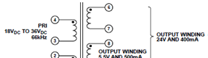
图6.变压器电路图

图7.评估板ADP1071-1EVALZ电路图
评估板ADP1071-1EVALZ材料清单:


图8.评估板ADP1071-1EVALZ PCB设计图(1):左:板尺寸;右:底层丝印

图9.评估板ADP1071-1EVALZ PCB设计图(2):左:顶层丝印;右:顶层布局

图10.评估板ADP1071-1EVALZ PCB设计图(3):左:层2;右:层4

图11.评估板ADP1071-1EVALZ PCB设计图(4):层3
评估板ADP1071-2EBZ3.3V
The ADP1071-2EBZ3.3V evaluation board allows users to evaluate the ADP1071-2 in a power supply application.
The ADP1071-2EBZ3.3V evaluation board is set up to act as an isolated power supply unit (PSU), with a rated load of 3.3 Vdc 3 A from a 36 Vdc to 60 Vdc source. There is also an auxiliary output of 8.0 Vdc, 10 mA. The operation of the converter is in continuous conduction mode (CCM).
All connectors and multiple test points allow easy access to all critical circuit nodes and pins of the ADP1071-2.
Multiple test points allow easy access to all critical circuit nodes and pins of the ADP1071-2.
Full data on the ADP1071-2 can be found in the ADP1071-2 data sheet, available from Analog Devices, Inc., which must be consulted in conjunction with this user guide when using the evaluation board.
评估板ADP1071-2EBZ3.3V主要特性:
Full support evaluation kit for the ADP1071-2
10 W flyback topology
3.3 V output voltage (Vdc)
3 A steady state
Auxiliary output of 8.0 Vdc, 10 mA
Forced CCM operation
Integrated drivers primary side MOSFET and secondary side synchronous rectifier
External reference signal tracking
Precision enable undervoltage lockout with hysteresis
Short-circuit, output overvoltage, and overtemperature protection
Cycle by cycle input overcurrent protection
Frequency synchronization
Soft start and soft stop functionality

图12.评估板ADP1071-2EBZ3.3V外形图

图13.评估板ADP1071-2EBZ3.3V框图

图14.评估板ADP1071-2EBZ3.3V电路图
评估板ADP1071-2EBZ3.3V材料清单:


责任编辑:HanFeng
【免责声明】
1、本文内容、数据、图表等来源于网络引用或其他公开资料,版权归属原作者、原发表出处。若版权所有方对本文的引用持有异议,请联系拍明芯城(marketing@iczoom.com),本方将及时处理。
2、本文的引用仅供读者交流学习使用,不涉及商业目的。
3、本文内容仅代表作者观点,拍明芯城不对内容的准确性、可靠性或完整性提供明示或暗示的保证。读者阅读本文后做出的决定或行为,是基于自主意愿和独立判断做出的,请读者明确相关结果。
4、如需转载本方拥有版权的文章,请联系拍明芯城(marketing@iczoom.com)注明“转载原因”。未经允许私自转载拍明芯城将保留追究其法律责任的权利。
拍明芯城拥有对此声明的最终解释权。
相关资讯
:
基于MC33771主控芯片的新能源锂电池管理系统解决方案

AMIC110 32位Sitara ARM MCU开发方案

基于AMIC110多协议可编程工业通信处理器的32位Sitara ARM MCU开发方案

基于展讯SC9820超低成本LTE芯片平台的儿童智能手表解决方案

基于TI公司的AM437x双照相机参考设计

基于MTK6580芯片的W2智能手表解决方案


 2012- 2022 拍明芯城ICZOOM.com 版权所有 客服热线:400-693-8369 (9:00-18:00)