基于Microchip公司PIC32MK 32位通用和马达控制MCU解决方案
 213
213
 拍明
拍明
原标题:Microchip PIC32MK 32位通用和马达控制MCU解决方案
Microchip公司的PIC32MKGP/MC系列是集成了FPU 32位通用和马达控制应用MCU,基于MIPS32® microAptiv™ MCU核,具有120MHz性能和高达1MB闪存, 256KB SRAM, 4KB EEPROM和运放,以及丰富外设,工作电压2.2V-3.6V,主要用在马达控制,工业控制和工业物联网(IIoT)以及多路CAN应用.本文介绍了PIC32MKGP/MC系列主要特性,框图,MIPS32® microAptiv™ MCU核主要特性和框图以及开发板DM320106主要特性,框图和电路图.
PIC32MK family devices combine 32-Bit, 120Mhz performance with up to 1MB of Flash memory, and a rich peripheral set targeting applications such as motor control, industrial control and Industrial Internet of Things (IIoT) and multi-channel CAN applications.
PIC32MKGP/MC系列主要特性:
Operating Conditions: 2.2V to 3.6V
•-40ºC to +105ºC, DC to 120 MHz
•-40ºC to +125ºC, DC to 80 MHz
Core: 120 MHz (up to 198 DMIPS)
•MIPS32® microAptiv™ MCU core with Floating Point Unit
•microMIPS™ mode for up to 40% smaller code size
•DSP-enhanced core:
-Four 64-bit accumulators
-Single-cycle MAC, saturating and fractional math
•Code-efficient (C and Assembly) architecture
•Two 32-bit core register files to reduce interrupt latency
Clock Management
•8 MHz ±2% (FRC) internal oscillator -40ºC to +85ºC
•Programmable PLLs and oscillator clock sources:
-HS and EC clock modes
•Secondary USB PLL
•32 kHz Internal Low-power RC oscillator (LPRC)
•Independent external low-power 32 kHz crystal oscillator
•Fail-Safe Clock Monitor (FSCM)
•Independent Watchdog Timers (WDT) and Deadman Timer (DMT)
•Fast wake-up and start-up
•Four Fractional clock out (REFCLKO) modules
Power Management
•Low-power management modes (Deep Sleep, Sleep, and Idle)
•Integrated:
-Power-on Reset (POR) and Brown-out Reset (BOR)
•On-board capacitorless regulator
Motor Control PWM
•Eight PWM pairs
•Six additional Single-Ended PWM modules
•Dead Time for rising and falling edges
•Dead-Time Compensation
•8.33 ns PWM Resolution
•Clock Chopping for High-frequency Operation
•PWM Support for:
-DC/DC, AC/DC, inverters, PFC, lighting
-BLDC, PMSM, ACIM, SRM motors
•Choice of six Fault and Current Limit Inputs
•Flexible Trigger Configuration for ADC Triggering
Motor Encoder Interface
•Six Quadrature Encoder Interface (QEI) modules:
-Four inputs: Phase A, Phase B, Home, and Index
Audio/Graphics/Touch Interfaces
•External Graphics interfaces through PMP
•Up to six I2S audio data communication interfaces
•Up to six SPI audio control interfaces
•Programmable audio master clock:
-Generation of fractional clock frequencies
-Can be synchronized with USB clock
-Can be tuned in run-time
Unique Features
•Permanent non-volatile 4-word unique device serial number
Direct Memory Access (DMA)
•Up to eight channels with automatic data size detection
•Programmable Cyclic Redundancy Check (CRC)
•Up to 64 KB transfers
Security Features
•Advanced Memory Protection:
-Peripheral and memory region access control
-Secure boot
Advanced Analog Features
•12-bit ADC module:
-25.45 Msps 12-bit mode or 33.79 Msps 8-bit mode
-7 individual ADC modules
-3.75 Msps per S&H with dedicated DMA
-Up to 42 analog inputs
•Flexible and independent ADC trigger sources
•Four Op amps and five Comparators
•Up to three 12-bit CDACs
•Internal temperature sensor ±2ºC accuracy
•Capacitive Touch Divider (CVD)
Communication Interfaces
•Up to four CAN modules (with dedicated DMA channels):
-2.0B Active with DeviceNet™ addressing support
•Up to six UART modules (up to 25 Mbps):
-Supports LIN 1.2 and IrDA® protocols
•Six SPI/I2S modules (SPI 50 Mbps)
•Parallel Master Port (PMP)
•Up to two FS USB 2.0-compliant On-The-Go (OTG) controllers
•Peripheral Pin Select (PPS) to enable remappable pin functions
Timers/Output Compare/Input Capture/RTCC
•Up to 14 16-bit or one 16-bit and eight 32-bit timers/counters for GP and MC devices and six additional QEI 32-bit timers for MC devices
•16 Output Compare (OC) modules
•16 Input Capture (IC) modules
•PPS to enable function remap
•Real-Time Clock and Calendar (RTCC) module
Input/Output
•5V-tolerant pins with up to 22 mA source/sink
•Selectable internal open drain, pull-ups, and pull-downs
•External interrupts on all I/O pins
•Five programmable edge/level-triggered interrupt pins
Qualification and Class B Support
•AEC-Q100 REVG (Grade 1 -40ºC to +125ºC) (planned)
•Class B Safety Library, IEC 60730 (planned)
•Back-up internal oscillator
•Clock monitor with back-up internal oscillator
•Global register locking
Debugger Development Support
•In-circuit and in-application programming
•2-wire or 4-wire MIPS® Enhanced JTAG interface
•Unlimited software and 12 complex breakpoints
•IEEE 1149.2-compatible (JTAG) boundary scan
•Non-intrusive hardware-based instruction trace
Software and Tools Support
•C/C++ compiler with native DSP/fractional support
•MPLAB® Harmony Integrated Software Framework
•TCP/IP, USB, Graphics, and mTouch™ middleware
•MFi, Android™ and Bluetooth® audio frameworks
•RTOS Kernels: Express Logic ThreadX, FreeRTOS™, OPENRTOS®, Micriμm® μC/OS™, and SEGGER embOS®
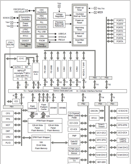
图1.PIC32MK GP/MC系列框图
The MIPS32® microAptiv™ MCU Core is the heart of the PIC32MK GP/MC family device processor. The CPU fetches instructions, decodes each instruction, fetches source operands, executes each instruction and writes the results of instruction execution to the proper destinations.
MIPS32® microAptiv™ MCU核主要特性:
•5-stage pipeline
•32-bit address and data paths
•MIPS32 Enhanced Architecture (Release 5):
-Multiply-accumulate and multiply-subtract instructions
-Targeted multiply instruction
-Zero/One detect instructions
-WAIT instruction
-Conditional move instructions (MOVN, MOVZ)
-Vectored interrupts
-Programmable exception vector base
-Atomic interrupt enable/disable
-GPR shadow registers to minimize latency for interrupt handlers
-Bit field manipulation instructions
-Virtual memory support
•microMIPS™ compatible instruction set:
-Improves code size density over MIPS32, while maintaining MIPS32 performance.
-Supports all MIPS32 instructions (except branch-likely instructions)
-Fifteen additional 32-bit instructions and 39 16-bit instructions corresponding to commonly-used MIPS32 instructions
-Stack pointer implicit in instruction
-MIPS32 assembly and ABI compatible
•Autonomous Multiply/Divide Unit (MDU):
-Maximum issue rate of one 32x32 multiply per clock
-Early-in iterative divide. Minimum 12 and maximum 38 clock latency (dividend (rs) sign extension-dependent)
•Power Control:
-Minimum frequency: 0 MHz
-Low-Power mode (triggered by WAIT instruction)
-Extensive use of local gated clocks
•EJTAG Debug and Instruction Trace:
-Support for single stepping
-Virtual instruction and data address/value breakpoints
-Hardware breakpoint supports both address match and address range triggering.
-Eight instruction and four data complex breakpoints
•iFlowtrace® version 2.0 support:
-Real-time instruction program counter
-Special events trace capability
-Two performance counters with 34 user-selectable countable events
-Disabled if the processor enters Debug mode
-Program Counter sampling
•DSP ASE Extension:
-Native fractional format data type operations
-Register Single Instruction Multiple Data (SIMD) operations (add, subtract, multiply, shift)
-GPR-based shift
-Bit manipulation
-Compare-Pick
-DSP Control Access
-Indexed-Load
-Branch
-Multiplication of complex operands
-Variable bit insertion and extraction
-Virtual circular buffers
-Arithmetic saturation and overflow handling
-Zero-cycle overhead saturation and rounding operations
•Floating Point Unit (FPU):
-1985 IEEE-754 compliant Floating Point Unit
-Supports single and double precision datatypes
-2008 IEEE-754 compatibility control of NaN handling and Abs/Neg instructions
-Runs at 1:1 core/FPU clock ratio
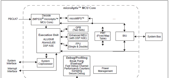
图2.PIC32MK GP/MC系列微处理器核框图
开发板DM320106
The PIC32MK GP Development Kit - DM320106 - offers a low cost solution for developers looking to build projects with the PIC32MK series of devices, featuring a rich assortment of CAN, USB, ADC and GPIO type inputs. This board also includes a SolomanSystec SSD1963 graphics driver and 30-Pin connector to enable graphics applications with available LCD panels.
The PIC32MK General Purpose (GP) Development Board provides a low-cost method for the development and testing of CAN, USB, and other applications with PIC32MK GP devices.
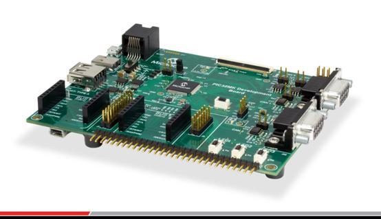
图3.开发板DM320106外形图
开发板DM320106主要特性:
• PIC32MK1024GPE-100: MIPS® MCU, 120MHz, DSP, FPU, 1MB Flash, 256KSRAM
• USB ports with Type-A, micro-B, and Type-C connectors
• 4-channel CAN Support through two DB9 connectors and two pin-headers
• Dual mikroBUS Click™ headers
• Solomon Systech SSD1963 Embedded Display SRAM LCD Controller with 50-Pinconnector
• 30-pin general purpose header
• On-board debugger or programmer interface (through PKOB, REAL ICE3™, andMPLAB® ICD3)
开发板DM320106包括:
• PIC32MK GP Development Board
• Type-A to micro-B USB cable
详情请见:
责任编辑:HanFeng
【免责声明】
1、本文内容、数据、图表等来源于网络引用或其他公开资料,版权归属原作者、原发表出处。若版权所有方对本文的引用持有异议,请联系拍明芯城(marketing@iczoom.com),本方将及时处理。
2、本文的引用仅供读者交流学习使用,不涉及商业目的。
3、本文内容仅代表作者观点,拍明芯城不对内容的准确性、可靠性或完整性提供明示或暗示的保证。读者阅读本文后做出的决定或行为,是基于自主意愿和独立判断做出的,请读者明确相关结果。
4、如需转载本方拥有版权的文章,请联系拍明芯城(marketing@iczoom.com)注明“转载原因”。未经允许私自转载拍明芯城将保留追究其法律责任的权利。
拍明芯城拥有对此声明的最终解释权。


 产品分类
产品分类




 2012- 2022 拍明芯城ICZOOM.com 版权所有 客服热线:400-693-8369 (9:00-18:00)


