基于Maxim公司的MAX32620-1、MAX16813高性能超低功耗MCU可充电设备开发方案
 403
403
 拍明
拍明
原标题:Maxim MAX32620-1高性能超低功耗MCU可充电设备开发方案
Maxim公司的MAX32620/MAX32621是带有FPU的高性能超低功耗的32位RISCARM® Cortex®-M4内核的微控制器,内部的96MHz提供了高性能,而4MHz振荡器支持需要经常监视的应用时的最小化功耗. 器件集成了2MB/1MB闪存,256KB SRAM,8KB指令缓存,核电压1.2V,1.8V-3.3V I/O,主要用在体育用手表,健身监视器,可穿戴医疗设备,手持媒体播放器和传感器集线器.本文介绍了MAX32620/MAX32621主要优势和特性,框图和可穿戴应用电路,以及评估板MAX32620 EVK主要优势和特性,框图,电路图和材料清单.
The MAX32620/MAX32621 is a 32-bit RISC ARM® Cortex®-M4 with FPU-based microcontroller. It is ideally suited for the emerging category of medical and fitness applications. The architecture combines high-efficiency, signal-processing functionality with low cost, and ease of use. An internal 96MHz oscillator provides high-performance capability, and the internal 4MHz oscillator supports minimal power consumption for applications requiring always-on monitoring.
The device features 4 powerful & flexible power modes. Built-in dynamic clock gating and firmware controlled power gating minimize power consumption for any application.Multiple SPI, UART, and I2C serial interfaces, as well as a 1-Wire® master and USB, interconnect to a wide variety of external sensors.
A four-input, 10-bit ADC with selectable references is provided.The MAX32621 is a secure version of the MAX32620. It incorporates a trust protection unit (TPU) with encryption and advanced security features. These features include a modular arithmetic accelerator (MAA) for ECDSA, a true random number generator (TRNG), and a secure boot loader. Both the MAX32620 and the MAX32621 provide a hardware AES engine.
The MAX32620L is a reduced memory version of the MAX32620, providing 1MB of flash memory and 256kB of SRAM.The enhanced features described in this data sheet apply to C and later revisions of the device. The MAX32620/MAX32621 supports a legacy mode making it compatible with first generation (revision A) of the device.
MAX32620/MAX32621主要优势和特性:
High-Efficiency Microcontroller for Wearable DevicesInternal Oscillator Operates Up to 96MHz
Low Power 4MHz Option for Always-On Monitoring
2MB/1MB Flash Memory
256KB SRAM
8KB Instruction Cache
1.2V Core Supply Voltage
1.8V to 3.3V I/O
Optional 3.3V ±5% USB Supply Voltage
Wide Operating Temperature: -30℃ to +85℃
Power Management Maximizes Uptime for Battery Applications122μW/MHz Active Executing from Cache
62μW/MHz Active Executing from Flash
Wake-Up to 96MHz Clock or 4MHz Clock
1.06μW Low Power Mode (LP0) Mode with RTC
2.67μW Ultra-Low Power Data Retention Sleep Mode (LP1) with Fast 5μs (typ) Wakeup on 96MHz
28μW/MHz Low Power Mode (LP2) Current
Optimal Peripheral Mix Provides Platform Scalability Three SPI Masters, One SPI Slave
Four UARTs
Up to Three I2C Masters, One I2C Slave
1-Wire® Master
Up to 49 General-Purpose I/O Pins
SPI Execute in Place (SPIX) Engine for Memory Expansion with Minimal Footprint
Full-Speed USB 2.0 with Internal Transceiver
Sixteen Pulse Train Engines
Six 32-Bit or 12 16-Bit Timers
Three Watchdog Timers with Independent Sources
Four-Input, 10-Bit Sigma-Delta ADC Operating at 7.8kS/s, 5.5V, and 1.8V Tolerant Inputs
AES-128, -192, -256 Hardware Engine
CMOS-Level 32kHz RTC Output Option
JTAG 1149.1 Compatible with Serial Wire Debug
Secure Valuable IP and Data with Robust Internal Hardware Security (MAX32621 Only)Trust Protection Unit (TPU) Provides ECDSA and Modular Arithmetic Acceleration Support
True Random Number Generator (TRNG)
Secure Boot Loader
MAX32620/MAX32621应用:
Sport Watches
Fitness Monitors
Wearable Medical Patches
Portable Medical Devices
Sensor Hub
评估板MAX32620 EVK
The MAX32620 and MAX32621 evaluation kits (EV kits) provide a convenient platform for evaluating the capabilities of the MAX32620 and MAX32621 microcontrollers, respectively. While the MAX32620 EV kit includes a MAX32620 soldered directly to the board, the MAX32621 EV kit features a socketed MAX32621. Each EV kit also provides a complete, functional system ideal for development and debugging applications. Except where stated otherwise, the following sections apply to both EV kits.
评估板MAX32620 EVK主要优势和特性:
Easily Load and Debug Code Using the Supplied Olimex ARM-USB-TINY-H JTAG Debugger Connected Through a Standard 20-Pin ARM JTAG Header
Headers for Accessing the IC’s Pins and Analog Front End (AFE) Input Signals
Micro-USB Type-B Connection to the IC’s USB Device Controller
Micro-USB Type-B Connection to USB-UART Bridge Selectable Between the IC’s Internal UART 0 and UART 1 On-Board Bluetooth® 4.0 BLE Transceiver with Chip Antenna
评估板MAX32620 EVK包括:
EV Kit Board with a MAX32620 Soldered Down (MAX32620 EV Kit Only)
EV Kit Board with a Socketed MAX32621 (MAX32621 EV Kit Only)
Olimex ARM-USB-TINY-H JTAG Debugger with JTAG Ribbon Cable (for Connecting from Debugger to EV Kit Header J1) and USB Standard A-to-B cable (for Connecting from PC to Debugger)
Two Standard-A to Micro-B USB Cables (for Connecting from a PC or Stand-Alone USB Power Supply to EV Kit Connectors CN1 and CN2)
MAX32620/MAX32621 EV Kit Quick Start
Hex Keys for the Socket (MAX32621 EV Kit Only)
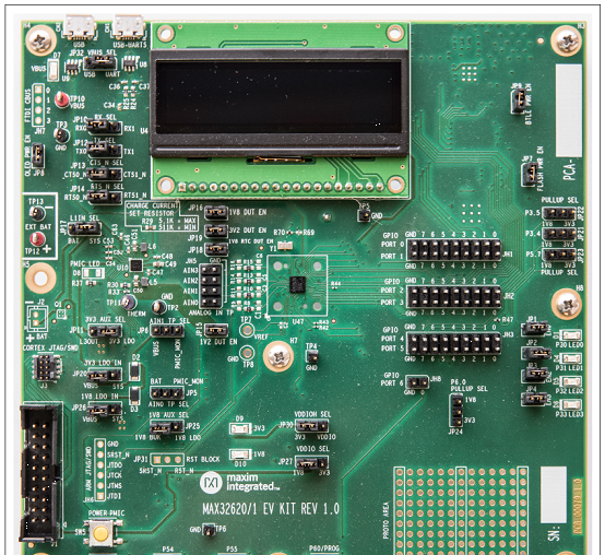
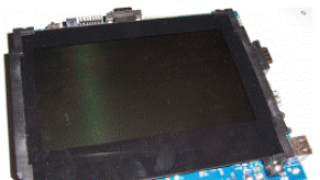
图.评估板MAX32620 EVK外形图
MAX16813
Description
The MAX16813 high-efficiency, high-brightness LED (HB LED) driver provides four integrated LED current-sink channels. An integrated current-mode switching controller drives a DC-DC converter that provides the necessary voltage to multiple strings of HB LEDs. The device accepts a wide 4.75V to 40V input voltage range and withstands direct automotive load-dump events. The wide input range allows powering HB LEDs for small- to medium-sized LCD displays in automotive and general lighting applications.
An internal current-mode switching DC-DC controller supports boost or SEPIC topologies and operates in an adjustable frequency range between 200kHz and 2MHz. An integrated spread-spectrum mode helps reduce EMI. Current-mode control with programmable slope compensation provides fast response and simplifies loop compensation. An adaptive output-voltage control scheme minimizes power dissipation in the LED current-sink paths. The device has a separate p-channel drive (PGATE) pin that is used for output undervoltage protection. Whenever the output falls below the threshold, the external p-MOSFET is latched off, disconnecting the input source. Cycling the EN or the input supply is required to restart the converter. The external p-MOSFET is off when the EN pin is below 0.3V (typ). The shutdown current is 1µA (typ) at an input voltage of 12V.
The device consists of four identical linear current-sink channels, adjustable from 20mA to 150mA with an accuracy of ±3% using a single external resistor. Multiple channels can be connected in parallel to achieve higher current per LED string. The device also features a unique pulsed dimming control through a logic input (DIM), with minimum pulse width as low as 500ns. Protection features include output overvoltage, open-LED detection and protection, programmable shorted LED detection and protection, output undervoltage protection and detection, and overtemperature protection. The device operates over the -40°C to +125°C automotive temperature range. The MAX16813 is available in 20-pin (6.5mm x 4.4mm) TSSOP and 20-pin (4mm x 4mm) TQFN packages.
MAX16813: Typical Operating Circuit
Enlarge+
Key Features
4-Channel Linear LED Current Sinks with Internal MOSFETs Independently Drive Multiple LED Strings
Full-Scale LED Current Adjustable from 20mA to 150mA
Drives 1 to 4 LED Strings
10000:1 PWM Dimming at 200Hz
Flexible Current-Mode Architecture Supports a Wide Range of Applications While Minimizing Interference
Boost or SEPIC Current-Mode DC-DC Controller
200kHz to 2MHz Programmable Switching Frequency
External Switching-Frequency Synchronization
Spread-Spectrum Mode
Protection Features Enhance Fault Detection and System Reliability
Output-to-Ground Undervoltage Protection
Open-Drain Fault-Indicator Output
Open-LED and LED-Short Detection and Protection
Overtemperature Protection
Adaptive Output-Voltage Optimization to Minimize Power Dissipation
Less than 2µA Shutdown Current
Applications/Uses
Architectural, Industrial, and Ambient Lighting
Automotive Displays LED Backlights
Automotive RCL, DRL, Front Position, and Fog Lights
LCD TV and Desktop Display LED Backlights
详情请见:
责任编辑:HanFeng
【免责声明】
1、本文内容、数据、图表等来源于网络引用或其他公开资料,版权归属原作者、原发表出处。若版权所有方对本文的引用持有异议,请联系拍明芯城(marketing@iczoom.com),本方将及时处理。
2、本文的引用仅供读者交流学习使用,不涉及商业目的。
3、本文内容仅代表作者观点,拍明芯城不对内容的准确性、可靠性或完整性提供明示或暗示的保证。读者阅读本文后做出的决定或行为,是基于自主意愿和独立判断做出的,请读者明确相关结果。
4、如需转载本方拥有版权的文章,请联系拍明芯城(marketing@iczoom.com)注明“转载原因”。未经允许私自转载拍明芯城将保留追究其法律责任的权利。
拍明芯城拥有对此声明的最终解释权。


 产品分类
产品分类




 2012- 2022 拍明芯城ICZOOM.com 版权所有 客服热线:400-693-8369 (9:00-18:00)


