


 产品分类
产品分类
基于Microchip公司MCP19214(5)两路模拟PWM电源控制方案
 198
198
 拍明
拍明
原标题:Microchip MCP19214(5)两路模拟PWM电源控制方案
Microchip公司的MCP19214/5是高度集成两路数字增强的PWM控制器,包括全可编微控制器核和10位模拟数字转换器(ADC);每个PWM通路包括两个误差放大器和单独可调基准电压发生器,电流检测输入,可编斜率补偿发生器,可编振荡器,电流差分放大器和MOSFET驱动器,输入电报压4.5V-42V,满足AEC Q100规范和PPAP功能,主要用在双向电源转换器,LED照明系统,电池充电器和其它低边开关PWM应用.本文介绍了MCP19214/5主要特性和框图,MCU核框图,应用框图以及MCP19215 双路升压/SEPIC评估板主要特性,电路图,材料清单和PCB设计图.
The MCP19214/5 devices are highly integrated,digitally enhanced PWM controllers, used for batterychargers, bidirectional converters, LED lightingsystems and other low-side switch PWM applications.
These devices feature two independent analog PWMcontrollers, and the internal architecture is optimizedfor applications that require precise control of theoutput parameters. Like the other members of thedigitally enhanced PWM controllers family,MCP19214/5 includes a fully programmablemicrocontroller core and a 10-bit analog-to-digitalconverter.
Each PWM channel includes two error amplifiers withindependent adjustable reference voltage generators,current sense input with programmable leading edgeblanking, programmable slope compensation rampgenerator, integrated internal programmable oscillator,current sense differential amplifier and an integratedMOSFET driver.
An internal LDO (+5V) is used to power the PIC core,the analog circuitry and to provide 5V externally. This5V external output can also be used to supply theinternal MOSFET drivers. The internal MOSFETdrivers have the option to be powered from an external voltage source (up to 10V) in order to accommodateapplications that require higher voltages for gatedriving.
The MCP19214/5 controllers offer a very high degreeof integration, allowing the user to develop complexapplications without additional circuitry. Some uniquefeatures, like simultaneous control of the converter’soutput current and voltage, make MCP19214/5 devices ideally suited for battery chargers, LED driversand bidirectional converters. Additionally, the GeneralPurpose Inputs/Outputs (GPIOs) can be used to drivevarious switches, to enable/disable additional circuitry,or to indicate a typical state.The MCP19214 is packaged in a 28-lead5 mm x 5 mm QFN,and the MCP19215 in a 32-lead5 mm x 5 mm QFN. The operating input voltage fornormal device operation is 4.5V-42V, with an absolutemaximum of 44V. The maximum transient voltage is48V for 500 mS.Power trains supported by this architecture include, butare not limited to, Boost, Buck-Boost, Flyback, SEPICand Cuk.
MCP19214/5 integrates an I2C controller and anAddressable Universal Synchronous AsynchronousReceiver Transmitter (AUSART) module (only forMCP19215). The user can develop specificcommunication protocols using the internal interfaces.A PMBus compatible protocol, specific for powerconverters, can be implemented using the providedI2C serial bus.
Complete customization of the device operatingparameters, start-up or shutdown profiles, protectionlevels and fault handling procedures are accomplishedby firmware that can be developed using Microchip’sMPLAB® X Integrated Development Environment.Programming the MCP19214/5 is done using one ofMicrochip’s many in-circuit debugger and deviceprogrammers.
MCP19214/5主要特性:
• AEC Q100 Qualified and PPAP Capable
• Input Voltage Range: 4.5V-42V
• Two Independent High-Performance PWMControllers
• Two Independent Control Loops per Channelallowing the User to Simultaneously Control theOutput Voltage and Current
• Can Be Configured to Control Multiple Topologiesincluding but Not Limited To:
- Boost
- Flyback
- Ćuk
- Single-Ended Primary-Inductor Converter(SEPIC)
• Peak Current Mode Control
• Master/Slave Operation of the PWM Controllerswith Adjustable Phase Shift
• Differential Output Current Sense Capability
• Integrated Low-Side Current Sense DifferentialAmplifier (10X)
• Integrated Low-Side Gate Drivers:
- 0.5A Sink/Source Current Capability at 5VSupply Voltage
- 1A Sink/Source Current Capability at 10VSupply Voltage
• Special Events Generator (the state of regulatingloops can be monitored without firmwareoverhead)
• Configurable Parameters:
- Reference Voltages for Regulating Loops(four internal DACs)
- Input Undervoltage Lockout (UVLO)
- Input Overvoltage Lockout (OVLO)
- Primary Current Leading Edge Blanking:0 ns, 50 ns, 100 ns and 200 ns
- Fixed Switching frequency Range:31.25 kHz-2.0 MHz
- Slope Compensation
- Primary Current Sense Offset Adjustment
- Configurable GPIO Pin Options
• Low Quiescent Current: 10 mA Typical
• Low Sleep Current: 120 μA Typical
• Thermal Shutdown
Microcontroller Features
• Precision 8 MHz Internal Oscillator Block:
- Factory-Calibrated to ±1%, Typical
• Interrupt-Capable
- Firmware
- Interrupt-on-Change Pins
• Only 35 Instructions to Learn
• 8192 Words On-Chip Program Memory
• 336 bytes of Internal RAM
• High-Endurance Flash:
- 100,000 Write Flash Endurance
- Flash Retention: > 40 Years
• Watchdog Timer (WDT) with IndependentOscillator for Reliable Operation
• Programmable Code Protection
• In-Circuit Serial Programming™ (ICSP™) via TwoPins
• Up to 12 I/O Pins and One Input-Only Pin
• Analog-to-Digital Converter (ADC):
- 10-Bit Resolution
- Internal 4096 mV Precision ReferenceGenerator
- Up to 8 External Channels
• Timer0: 8-Bit Timer/Counter with 8-Bit Prescaler
• Enhanced Timer1:
- 16-bit Timer with Prescaler
- Two Selectable Clock Sources
• Timer2: 8-Bit Timer with Prescaler
- 8-Bit Period Register
• I2C Communication:
- 7-bit Address Masking
- Two Dedicated Address Registers
• Addressable Universal Synchronous
Asynchronous Receiver Transmitter (AUSART)(only MCP19215):
- 8 and 9-Bit Data Operations
- Address Detect
- Asynchronous and Synchronous OperatingModes
MCP19215 双路升压/SEPIC评估板
The MCP19215 Dual Boost/SEPIC Evaluation Board demonstrates how theMCP19215 device operates in Boost and SEPIC topologies over a wide input voltageand load range. Nearly all operational and control system parameters are programmableby utilizing the integrated PIC controller.
For precise measurements of output current, a 0.1 shunt is used on each channel.
Output current is measured using an internal op amp.
The Graphical User Interface (GUI) can be used to program the functioning
parameters, and check operational status. To simplify the connection, a USB-to-I2C
communication bridge is implemented on board, using the MCP2221-I/SL SOIC14-Lead, allowing standard interface to any Microsoft® Windows® computer.
Alternatively, users can program the MCP19215 using their own firmware, further tailoring
it to the application, using the MPLAB® X Integrated Development Environment(IDE) and a PICkit™ 3 Programmer/Debugger on the J5 Header.
The MCP19215 Dual Boost/SEPIC Evaluation Board board is equipped with headers
for In-Circuit Serial Programming™ (ICSP™), a mini-USB type B for communication,and test point pads on each GPIO pin.
The MCP19215 Dual Boost/SEPIC Evaluation Board is also intended to demonstrate
an optimized Printed Circuit Board (PCB) layout that minimizes parasitic noise while
increasing efficiency and power density. Proper PCB layout is critical to achieve optimum
MCP19215 operation, as well as power train efficiency and noise minimization.
The MCP19215 Dual Channel Controller Evaluation Board demonstrates how the MCP19215 device operates in Boost and SEPIC topologies over a wide input voltage and load range. Nearly all operational and control system parameters are programmable by utilizing the integrated PIC controller.
MCP19215 双路升压/SEPIC评估板主要特性:
• input voltage range: 8V to 15V
• output voltage: default 20V for both channels (can be software adjusted from input voltage + 1V to 24V for channel 1 and 9V to 24V for channel 2)
• default output current: 0.2A (can be software adjusted from 0A to 1A)
• 300 kHz switching frequency
• status report (including errors, input voltage, output voltage and current) via I2C communication
• under voltage lockout (UVLO) and overvoltage lockout (OVLO) with programmable thresholds (via software)
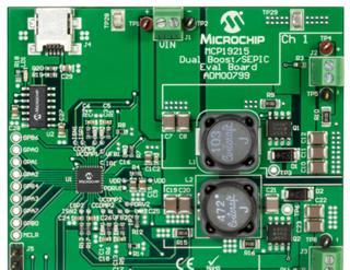
图.MCP19215 双路升压/SEPIC评估板外形图
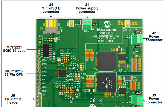
图.MCP19215 双路升压/SEPIC评估板顶层图
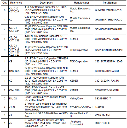
MCP19215 双路升压/SEPIC评估板材料清单:

详情请见:
责任编辑:Davia
【免责声明】
1、本文内容、数据、图表等来源于网络引用或其他公开资料,版权归属原作者、原发表出处。若版权所有方对本文的引用持有异议,请联系拍明芯城(marketing@iczoom.com),本方将及时处理。
2、本文的引用仅供读者交流学习使用,不涉及商业目的。
3、本文内容仅代表作者观点,拍明芯城不对内容的准确性、可靠性或完整性提供明示或暗示的保证。读者阅读本文后做出的决定或行为,是基于自主意愿和独立判断做出的,请读者明确相关结果。
4、如需转载本方拥有版权的文章,请联系拍明芯城(marketing@iczoom.com)注明“转载原因”。未经允许私自转载拍明芯城将保留追究其法律责任的权利。
拍明芯城拥有对此声明的最终解释权。
相关资讯
:
基于MC33771主控芯片的新能源锂电池管理系统解决方案

AMIC110 32位Sitara ARM MCU开发方案

基于AMIC110多协议可编程工业通信处理器的32位Sitara ARM MCU开发方案

基于展讯SC9820超低成本LTE芯片平台的儿童智能手表解决方案

基于TI公司的AM437x双照相机参考设计

基于MTK6580芯片的W2智能手表解决方案


 2012- 2022 拍明芯城ICZOOM.com 版权所有 客服热线:400-693-8369 (9:00-18:00)


