


 产品分类
产品分类
基于TI公司的TIDEP-0087电动汽车(EV)充电桩人机接口(HMI)应用方案
 2772
2772
 拍明
拍明
原标题:TI TIDEP-0087电动汽车(EV)充电桩人机接口(HMI)参考设计
TI公司的TIDEP-0087是采用AM335x系列微处理器的电动汽车( EV)充电基础设施人机接口(HMI)参考设计,采用软件加速图像和Qt电阻触摸屏,4.3吋LCD支持480x272分辨率,其它显示器可升级2048x2048,主要用在电动汽车(EV)充电桩HMI模块.本文介绍AM335x系列微处理器主要特性和功能框图,参考设计TIDEP-0087主要特性和框图,以及TMDSSK3358评估板电路图和材料清单.
The AM335x microprocessors, based on the ARM Cortex-A8 processor, are enhanced with image,graphics processing, peripherals and industrial interface options such as EtherCAT and PROFIBUS. Thedevices support high-level operating systems (HLOS). Linux® and Android™ are available free of chargefrom TI.
The AM335x microprocessor contain the subsystems shown in Figure 1 and a brief description of eachfollows:
The microprocessor unit (MPU) subsystem is based on the ARM Cortex-A8 processor and the PowerVRSGX™ Graphics Accelerator subsystem provides 3D graphics acceleration to support display and gamingeffects.
The PRU-ICSS is separate from the ARM core, allowing independent operation and clocking for greaterefficiency and flexibility. The PRU-ICSS enables additional peripheral interfaces and real-time protocolssuch as EtherCAT, PROFINET, EtherNet/IP, PROFIBUS, Ethernet Powerlink, Sercos, and others.
Additionally, the programmable nature of the PRU-ICSS, along with its access to pins, events and allsystem-on-chip (SoC) resources, provides flexibility in implementing fast, real-time responses, specializeddata handling operations, custom peripheral interfaces, and in offloading tasks from the other processorcores of SoC.
AM335x系列主要特性:
• Up to 1-GHz Sitara™ ARM® Cortex®-A8 32‑BitRISC Processor
– NEON™ SIMD Coprocessor
– 32KB of L1 Instruction and 32KB of Data CacheWith Single-Error Detection (Parity)
– 256KB of L2 Cache With Error Correcting Code(ECC)
– 176KB of On-Chip Boot ROM
– 64KB of Dedicated RAM
– Emulation and Debug - JTAG
– Interrupt Controller (up to 128 InterruptRequests)
• On-Chip Memory (Shared L3 RAM)
– 64KB of General-Purpose On-Chip MemoryController (OCMC) RAM
– Accessible to All Masters
– Supports Retention for Fast Wakeup
• External Memory Interfaces (EMIF)
– mDDR(LPDDR), DDR2, DDR3, DDR3LController:
• mDDR: 200-MHz Clock (400-MHz DataRate)
• DDR2: 266-MHz Clock (532-MHz Data Rate)
• DDR3: 400-MHz Clock (800-MHz Data Rate)
• DDR3L: 400-MHz Clock (800-MHz DataRate)
• 16-Bit Data Bus
• 1GB of Total Addressable Space
• Supports One x16 or Two x8 Memory DeviceConfigurations
– General-Purpose Memory Controller (GPMC)
• Flexible 8-Bit and 16-Bit AsynchronousMemory Interface With up to Seven ChipSelects (NAND, NOR, Muxed-NOR, SRAM)
• Uses BCH Code to Support 4-, 8-, or 16-BitECC
• Uses Hamming Code to Support 1-Bit ECC
– Error Locator Module (ELM)
• Used in Conjunction With the GPMC toLocate Addresses of Data Errors from
Syndrome Polynomials Generated Using aBCH Algorithm
• Supports 4-, 8-, and 16-Bit per 512-ByteBlock Error Location Based on BCH
Algorithms
• Programmable Real-Time Unit Subsystem andIndustrial Communication Subsystem (PRU-ICSS)
– Supports Protocols such as EtherCAT®,PROFIBUS, PROFINET, EtherNet/IP™, and
More
– Two Programmable Real-Time Units (PRUs)
• 32-Bit Load/Store RISC Processor Capableof Running at 200 MHz
• 8KB of Instruction RAM With Single-ErrorDetection (Parity)
• 8KB of Data RAM With Single-ErrorDetection (Parity)
• Single-Cycle 32-Bit Multiplier With 64-BitAccumulator
• Enhanced GPIO Module Provides Shift-In/Out Support and Parallel Latch on
External Signal
– 12KB of Shared RAM With Single-ErrorDetection (Parity)
– Three 120-Byte Register Banks Accessible byEach PRU
– Interrupt Controller (INTC) for Handling SystemInput Events
– Local Interconnect Bus for Connecting Internaland External Masters to the Resources Insidethe PRU-ICSS
– Peripherals Inside the PRU-ICSS:
• One UART Port With Flow Control Pins,Supports up to 12 Mbps
• One Enhanced Capture (eCAP) Module
• Two MII Ethernet Ports that SupportIndustrial Ethernet, such as EtherCAT
• One MDIO Port
• Power, Reset, and Clock Management (PRCM)Module
– Controls the Entry and Exit of Stand-By andDeep-Sleep Modes
– Responsible for Sleep Sequencing, PowerDomain Switch-Off Sequencing, Wake-Up
Sequencing, and Power Domain Switch-OnSequencing
– Clocks
• Integrated 15- to 35-MHz High-FrequencyOscillator Used to Generate a Reference
Clock for Various System and PeripheralClocks
• Supports Individual Clock Enable andDisable Control for Subsystems andPeripherals to Facilitate Reduced PowerConsumption
• Five ADPLLs to Generate System Clocks(MPU Subsystem, DDR Interface, USB and
Peripherals [MMC and SD, UART, SPI, I2C],L3, L4, Ethernet, GFX [SGX530], LCD Pixel
Clock)
– Power
• Two Nonswitchable Power Domains (Real-Time Clock [RTC], Wake-Up Logic
[WAKEUP])
• Three Switchable Power Domains (MPUSubsystem [MPU], SGX530 [GFX],
Peripherals and Infrastructure [PER])
• Implements SmartReflex™ Class 2B forCore Voltage scaling Based On Die
Temperature, Process Variation, andPerformance (Adaptive Voltage Scaling
[AVS])
• Dynamic Voltage Frequency Scaling (DVFS)
• Real-Time Clock (RTC)
– Real-Time Date (Day-Month-Year-Day of Week)and Time (Hours-Minutes-Seconds) Information
– Internal 32.768-kHz Oscillator, RTC Logic and1.1-V Internal LDO
– Independent Power-on-Reset(RTC_PWRONRSTn) Input
– Dedicated Input Pin (EXT_WAKEUP) forExternal Wake Events
– Programmable Alarm Can be Used to GenerateInternal Interrupts to the PRCM (for Wakeup) orCortex-A8 (for Event Notification)
– Programmable Alarm Can be Used WithExternal Output (PMIC_POWER_EN) to Enablethe Power Management IC to Restore Non-RTCPower Domains
• Peripherals
– Up to Two USB 2.0 High-Speed OTG PortsWith Integrated PHY
– Up to Two Industrial Gigabit Ethernet MACs (10,100, 1000 Mbps)
• Integrated Switch
• Each MAC Supports MII, RMII, RGMII, andMDIO Interfaces
• Ethernet MACs and Switch Can OperateIndependent of Other Functions
• IEEE 1588v2 Precision Time Protocol (PTP)
– Up to Two Controller-Area Network (CAN) Ports
• Supports CAN Version 2 Parts A and B
– Up to Two Multichannel Audio Serial Ports(McASPs)
• Transmit and Receive Clocks up to 50 MHz
• Up to Four Serial Data Pins per McASP PortWith Independent TX and RX Clocks
• Supports Time Division Multiplexing (TDM),Inter-IC Sound (I2S), and Similar Formats
• Supports Digital Audio InterfaceTransmission (SPDIF, IEC60958-1, andAES-3 Formats)
• FIFO Buffers for Transmit and Receive (256Bytes)
– Up to Six UARTs
• All UARTs Support IrDA and CIR Modes
• All UARTs Support RTS and CTS FlowControl
• UART1 Supports Full Modem Control
– Up to Two Master and Slave McSPI SerialInterfaces
• Up to Two Chip Selects
• Up to 48 MHz
– Up to Three MMC, SD, SDIO Ports
• 1-, 4- and 8-Bit MMC, SD, SDIO Modes
• MMCSD0 has Dedicated Power Rail for
1.8‑V or 3.3-V Operation
• Up to 48-MHz Data Transfer Rate
• Supports Card Detect and Write Protect
• Complies With MMC4.3, SD, SDIO 2.0Specifications
– Up to Three I2C Master and Slave Interfaces
• Standard Mode (up to 100 kHz)
• Fast Mode (up to 400 kHz)
– Up to Four Banks of General-Purpose I/O(GPIO) Pins
• 32 GPIO Pins per Bank (Multiplexed WithOther Functional Pins)
• GPIO Pins Can be Used as Interrupt Inputs(up to Two Interrupt Inputs per Bank)
– Up to Three External DMA Event Inputs that canAlso be Used as Interrupt Inputs
– Eight 32-Bit General-Purpose Timers
• DMTIMER1 is a 1-ms Timer Used forOperating System (OS) Ticks
• DMTIMER4–DMTIMER7 are Pinned Out
– One Watchdog Timer
– SGX530 3D Graphics Engine
• Tile-Based Architecture Delivering up to 20Million Polygons per Second
• Universal Scalable Shader Engine (USSE) isa Multithreaded Engine Incorporating Pixel
and Vertex Shader Functionality
• Advanced Shader Feature Set in Excess ofMicrosoft VS3.0, PS3.0, and OGL2.0
• Industry Standard API Support of Direct3DMobile, OGL-ES 1.1 and 2.0, OpenVG 1.0,
andOpenMax
• Fine-Grained Task Switching, LoadBalancing, and Power Management
• Advanced Geometry DMA-Driven Operationfor Minimum CPU Interaction
• Programmable High-Quality Image Anti-Aliasing
• Fully Virtualized Memory Addressing for OSOperation in a Unified Memory Architecture
– LCD Controller
• Up to 24-Bit Data Output; 8 Bits per Pixel(RGB)
• Resolution up to 2048 × 2048 (WithMaximum 126-MHz Pixel Clock)
• Integrated LCD Interface Display Driver(LIDD) Controller
• Integrated Raster Controller
• Integrated DMA Engine to Pull Data from theExternal Frame Buffer Without Burdening theProcessor via Interrupts or a Firmware Timer
• 512-Word Deep Internal FIFO
• Supported Display Types:
– Character Displays - Uses LIDDController to Program these Displays
– Passive Matrix LCD Displays - Uses LCDRaster Display Controller to ProvideTiming and Data for Constant GraphicsRefresh to a Passive Display
– Active Matrix LCD Displays – UsesExternal Frame Buffer Space and theInternal DMA Engine to Drive StreamingData to the Panel
– 12-Bit Successive Approximation Register(SAR) ADC
• 200K Samples per Second
• Input can be Selected from any of the EightAnalog Inputs Multiplexed Through an 8:1
Analog Switch
• Can be Configured to Operate as a 4-Wire,5-Wire, or 8-Wire Resistive Touch Screen
Controller (TSC) Interface
– Up to Three 32-Bit eCAP Modules
• Configurable as Three Capture Inputs orThree Auxiliary PWM Outputs
– Up to Three Enhanced High-Resolution PWMModules (eHRPWMs)
• Dedicated 16-Bit Time-Base Counter WithTime and Frequency Controls
• Configurable as Six Single-Ended, Six Dual-Edge Symmetric, or Three Dual-Edge
Asymmetric Outputs
– Up to Three 32-Bit Enhanced QuadratureEncoder Pulse (eQEP) Modules
• Device Identification
– Contains Electrical Fuse Farm (FuseFarm) ofWhich Some Bits are Factory Programmable
• Production ID
• Device Part Number (Unique JTAG ID)
• Device Revision (Readable by Host ARM)
• Debug Interface Support
– JTAG and cJTAG for ARM (Cortex-A8 andPRCM), PRU-ICSS Debug
– Supports Device Boundary Scan
– Supports IEEE 1500
• DMA
– On-Chip Enhanced DMA Controller (EDMA) hasThree Third-Party Transfer Controllers (TPTCs)and One Third-Party Channel Controller(TPCC), Which Supports up to 64
Programmable Logical Channels and EightQDMA Channels. EDMA is Used for:
• Transfers to and from On-Chip Memories
• Transfers to and from External Storage(EMIF, GPMC, Slave Peripherals)
• Inter-Processor Communication (IPC)
– Integrates Hardware-Based Mailbox for IPC andSpinlock for Process Synchronization BetweenCortex-A8, PRCM, and PRU-ICSS
• Mailbox Registers that Generate Interrupts
– Four Initiators (Cortex-A8, PRCM, PRU0,PRU1)
• Spinlock has 128 Software-Assigned LockRegisters
• Security
– Crypto Hardware Accelerators (AES, SHA,RNG)
– Secure Boot
• Boot Modes
– Boot Mode is Selected Through BootConfiguration Pins Latched on the Rising Edge
of the PWRONRSTn Reset Input Pin• Packages:
– 298-Pin S-PBGA-N298 Via Channel Package(ZCE Suffix), 0.65-mm Ball Pitch
– 324-Pin S-PBGA-N324 Package(ZCZ Suffix), 0.80-mm Ball Pitch
AM335x系列应用:
• Gaming Peripherals
• Home and Industrial Automation
• Consumer Medical Appliances
• Printers
• Smart Toll Systems
• Connected Vending Machines
• Weighing Scales
• Educational Consoles
• Advanced Toys
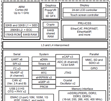
图1.AM335x系列功能框图
EV充电基础设施人机接口(HMI)参考设计TIDEP-0087
This processor-based reference design facilitates a quicker time to market and helps customers design cost-effective, human machine interface (HMI) solutions for electric vehicle (EV) charging infrastructure or EV supply equipment (EVSE). This reference design showcases a two-dimensional (2-D) Qt graphical user interface (GUI), which is typical for EVSE HMI, along with TI processor capabilities for software-rendered graphics. The AM335x processors provide scalability with various processing speeds, compatible software to satisfy low-to high-end applications, and ample connectivity with the key peripherals required for EVSE HMI, such as universal asynchronous receiver/transmitter (UART) and CAN.
With increasing battery capacity and decreasing battery cost, electric vehicles are becoming moremainstream each day. The EVSE is an infrastructure element that supplies electric energy for therecharging of electric vehicles, such as plug-in electric vehicles, including electric cars, neighborhoodelectric vehicles, and plug-in hybrids.
The EVSE system consists of a power stage, some sort of central processing unit (CPU) such as amicrocontroller (MCU) or microprocessor (MPU), communication subsystems for both internal dataexchange and external communications, and an HMI.
The Sitara™ AM335x processor, which is one of the most popular processors for industrial HMIapplications, not only has the resources targeted for processing the user interface of a charging station,but the AM335x processor’s easy-to-use programming tools and portfolio of on-chip capabilities givedesigners a head start on EVSE development projects.
Based on the AM335x Starter Kit Evaluation Module (EVM), the TIDEP-0087 reference design is a quickstarting point for customers who want to design an EVSE HMI module or system for an EV charginginfrastructure.
The TI AM335x high-performance processors are based on the ARM® Cortex®-A8 core.These enhanced processors have rich peripherals and an advanced display capability, including 2-D and3-D acceleration to help customers design cost-effective EVSE HMIs. The devices support high-leveloperating systems (HLOS) such as Linux, which is available free of charge from TI. The devices offer anupgrade to systems based on lower-performance ARM cores, provide updated peripherals, and supportthe typical interfaces to connect to EV charging power stages, such as UART and CAN.
参考设计TIDEP-0087主要特性:
4 example screens of charging station options using software accelerated graphics and Qt
Resistive touchscreen enabled
Support for 480x272 resolution on included 4.3 inch LCD, but scalable up to 2048x2048 on other displays
Built on TI’s Processor SDK-Linux for scalability to other Sitara processors
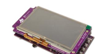
图2.参考设计TIDEP-0087外形图
参考设计TIDEP-0087应用:
EV Charging Station HMI Module
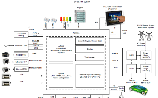
图3.参考设计TIDEP-0087 EVSE HMI框图
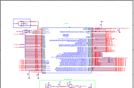
图4.TMDSSK3358评估板电路图(1)
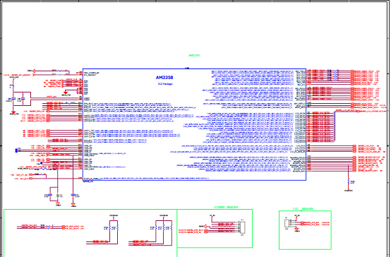
图5.TMDSSK3358评估板电路图(2)
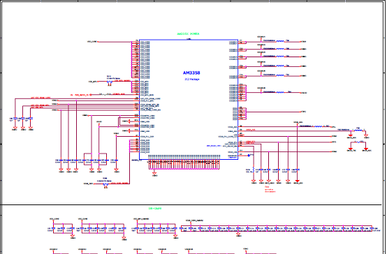
图6. TMDSSK3358评估板电路图(3)

图7. TMDSSK3358评估板电路图(4)
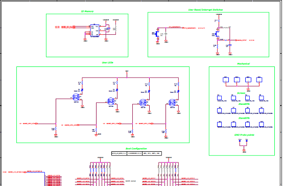
图8. TMDSSK3358评估板电路图(5)

图9. TMDSSK3358评估板电路图(6)

图10. TMDSSK3358评估板电路图(7)
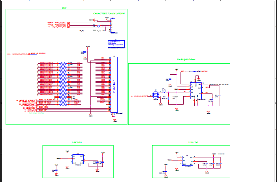
图11. TMDSSK3358评估板电路图(8)
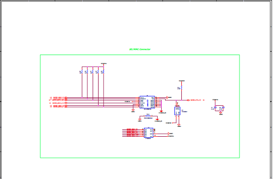
图12. TMDSSK3358评估板电路图(9)

图13. TMDSSK3358评估板电路图(10)
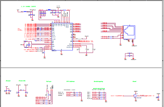
图14. TMDSSK3358评估板电路图(11)
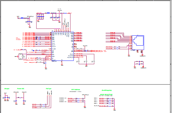
图15. TMDSSK3358评估板电路图(12)
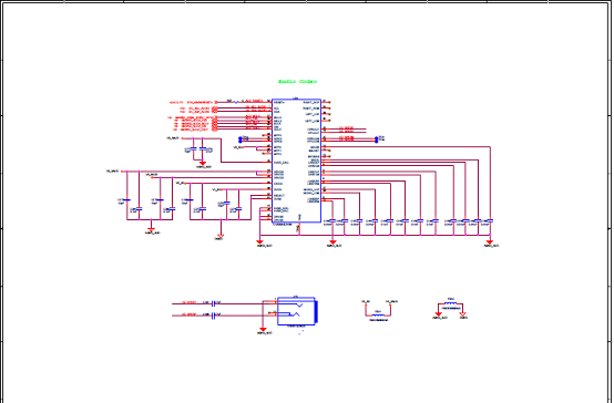
图16. TMDSSK3358评估板电路图(13)
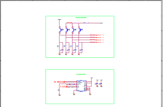
图17. TMDSSK3358评估板电路图(14)

图18. TMDSSK3358评估板电路图(15)
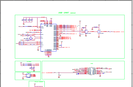
图19. TMDSSK3358评估板电路图(16)
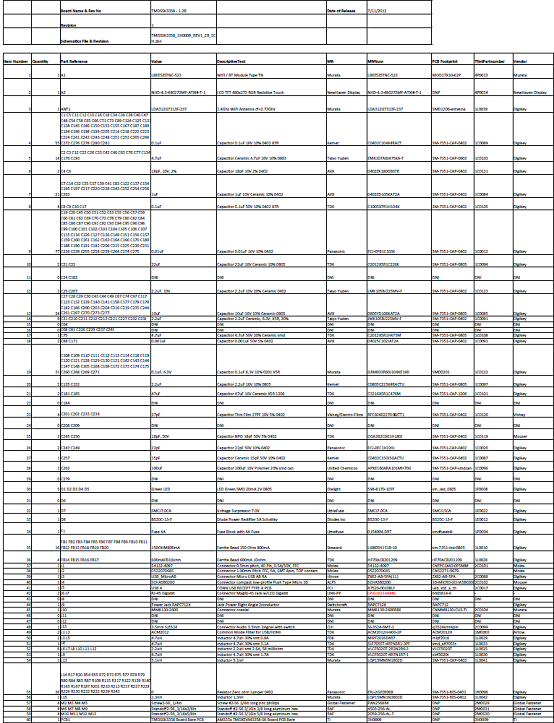
TMDSSK3358评估板材料清单:

详情请见:
责任编辑:Davia
【免责声明】
1、本文内容、数据、图表等来源于网络引用或其他公开资料,版权归属原作者、原发表出处。若版权所有方对本文的引用持有异议,请联系拍明芯城(marketing@iczoom.com),本方将及时处理。
2、本文的引用仅供读者交流学习使用,不涉及商业目的。
3、本文内容仅代表作者观点,拍明芯城不对内容的准确性、可靠性或完整性提供明示或暗示的保证。读者阅读本文后做出的决定或行为,是基于自主意愿和独立判断做出的,请读者明确相关结果。
4、如需转载本方拥有版权的文章,请联系拍明芯城(marketing@iczoom.com)注明“转载原因”。未经允许私自转载拍明芯城将保留追究其法律责任的权利。
拍明芯城拥有对此声明的最终解释权。
相关资讯
:
基于MC33771主控芯片的新能源锂电池管理系统解决方案

AMIC110 32位Sitara ARM MCU开发方案

基于AMIC110多协议可编程工业通信处理器的32位Sitara ARM MCU开发方案

基于展讯SC9820超低成本LTE芯片平台的儿童智能手表解决方案

基于TI公司的AM437x双照相机参考设计

基于MTK6580芯片的W2智能手表解决方案


 2012- 2022 拍明芯城ICZOOM.com 版权所有 客服热线:400-693-8369 (9:00-18:00)


