TI的LMG1210 200V半桥高性能氮化镓场效应晶体管电源参考设计TIDA-01634
 449
449
 拍明
拍明
TI公司的LMG1210是200V半桥高性能氮化镓场效应晶体管(GaN FET)驱动器,超高速度可到50MHz,传输时延10ns,脉冲宽度≥ 3 ns,高边和低边匹配1.5ns,峰值源电流1.5A,主要用在高速DC/DC转换器,RF包络跟踪,D类音频放大器和E类无线充电.本文介绍了LMG1210主要特性,框图和应用框图,以及高速DC/DC转换器GaN电流级参考设计TIDA-01634主要特性,框图以及主要指标,电路图,材料清单和PCB设计图.
The LMG1210 is a 200-V, half-bridge highperformance gallium nitride field effect transistor(GaN FET) driver designed for applications requiringhigh switching speed, minimized dead time, as wellas high efficiency. Drive voltage is preciselycontrolled by an internal LDO to 5 V when higherauxiliary voltages are used.
The LMG1210 GaN driver is designed for ultra-highfrequency applications and features adjustable deadtimecapability, very small propagation delay, as wellas 1.5-ns high-side low-side matching to optimizesystem efficiency.
Additional parasitic capacitance across the GaN FETis minimized to less than 1 pF to reduce additionalswitching losses. An external bootstrap diode is usedto charge the high-side bootstrap capacitor to allowoptimal selection for the circuit operating conditions.
An internal switch turns the bootstrap diode off whenthe low side is not on, effectively preventing the highsidebootstrap from overcharging and minimizing thereverse recovery charge when a silicon diode is usedas the bootstrap diode.
LMG1210主要特性:
1• Ultra-High Speed Operation of 50 MHz
– 10 ns Typical Propagation Delay
– 1.5 ns High-Side to Low-Side Matching
– Pulse Width ≥ 3 ns
• 1.5-A Peak Source and 3.1-A Peak Sink Currents
• Adjustable Dead-Time Control Feature
• Highest Slew Rate Immunity in Industry of 300V/ns
• External Bootstrap Diode For Flexibility
• High-Side to Low-Side Capacitance Less Than 1pF
• UVLO and Overtemperature Protection
• Low-Inductance WQFN Package
LMG1210应用:
• High-Speed DC-DC Converters
• RF Envelope Tracking
• Class-D Audio Amplifiers
• Class-E Wireless Charging
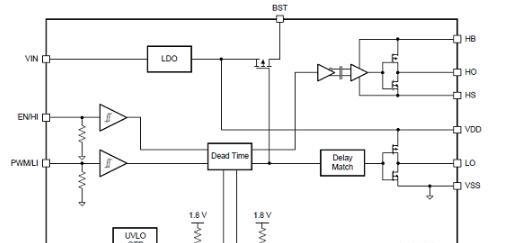
图1.LMG1210功能框图
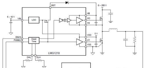
图2.LMG1210同步降压转换器简化电路图
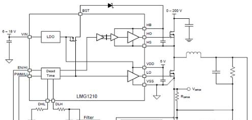
图3.LMG1210采用CMC滤波器带电流检测电阻配置图
高速DC/DC转换器GaN电流级参考设计TIDA-01634
This reference design implements a multi-MHz powerstage design based on the LMG1210 half-bridge GaNdriver and GaN power HEMTs. With highly efficientswitches and flexible dead-time adjustment, thisdesign can significantly improve power density whileachieving good efficiency as well as wide controlbandwidth. This power stage design can be widelyapplied to many space-constrained and fast responserequired applications such as 5G telecom power,servers, and industrial power supplies.
Switching-mode power supply designers are always pursing higher power density, which requires higherfrequency and efficiency. Compared to silicon FETs, gallium nitride (GaN) and high electron mobilitytransistors (HEMTs) exhibit a lower figure of merit, smaller gate charge, faster switching, and no reverserecovery loss.
This reference design uses GaN power HEMTs and the LMG1210 GaN half-bridge driver to realize amulti-MHz power stage with high efficiency. The half-bridge driver allows a single PWM input withconfigurable dead time or two independent inputs for high-side and low-side gate drive. Dead-timeadjustment can be realized with two resistors for low-to-high and high-to-low transition settings from 0 nsto 20 ns. In addition, the bootstrap switching action also prevents overvoltage of high-side gate due tolarge third quadrant voltage drop of GaN HEMTs.
This power stage can realize 3 ns of minimum on-time and up to a 50-MHz operation frequency. Thisdesign can stand a slew rate of 300 V/ns of common mode transient and provides driver UVLO andovertemperature protection.
This design can be applied to many space-constrained and fast response required applications such as5G telecom power, 48-to-POL server power, and industrial power supplies
参考设计TIDA-01634主要特性:
• Compact GaN-Based Power Stage Design WithSwitching up to 50 MHz
• Independent PWM Inputs for High Side andLow Side, or Single PWM Input WithAdjustableDead Time
• Minimum Pulse Width of 3 ns
• High Slew Rate Immunity of 300 V/ns
• Driver UVLO and Overtemperature Protection
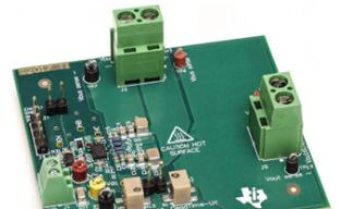
图4.参考设计TIDA-01634外形图
参考设计TIDA-01634应用:
• High-Speed, Synchronous Buck Converters
• Envelope Tracking
• Class D Audio Amplifiers
• Server and Network Power Supplies
• Industrial Power Supplies

图5.参考设计TIDA-01634框图
参考设计TIDA-01634主要指标:

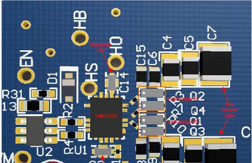
图6.参考设计TIDA-01634 PCB布局图
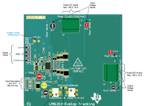
图7.参考设计TIDA-01634外形图
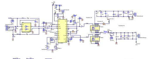
图8.参考设计TIDA-01634电路图
参考设计TIDA-01634材料清单:
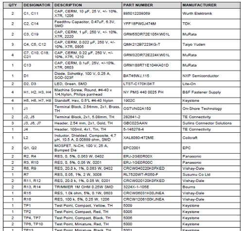
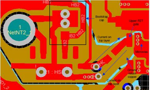
图9.参考设计TIDA-01634高边FET栅驱动回路布局图

图10.参考设计TIDA-01634 PCB设计图:左:并行FET栅驱动通路;右:并行FET栅驱动回程路
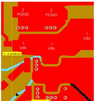
图11.参考设计TIDA-01634 PCB设计图:半桥电源回路布局
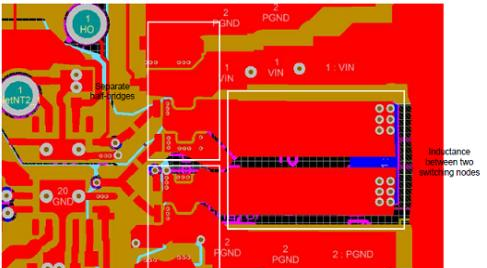
图12.参考设计TIDA-01634 PCB设计图:并行半桥对称电源回路布局
责任编辑:Davia
【免责声明】
1、本文内容、数据、图表等来源于网络引用或其他公开资料,版权归属原作者、原发表出处。若版权所有方对本文的引用持有异议,请联系拍明芯城(marketing@iczoom.com),本方将及时处理。
2、本文的引用仅供读者交流学习使用,不涉及商业目的。
3、本文内容仅代表作者观点,拍明芯城不对内容的准确性、可靠性或完整性提供明示或暗示的保证。读者阅读本文后做出的决定或行为,是基于自主意愿和独立判断做出的,请读者明确相关结果。
4、如需转载本方拥有版权的文章,请联系拍明芯城(marketing@iczoom.com)注明“转载原因”。未经允许私自转载拍明芯城将保留追究其法律责任的权利。
拍明芯城拥有对此声明的最终解释权。


 产品分类
产品分类




 2012- 2022 拍明芯城ICZOOM.com 版权所有 客服热线:400-693-8369 (9:00-18:00)


