TI LMG341xR070 GaN双向CCM图腾柱PFC参考设计TIDM-02008
 280
280
 拍明
拍明
原标题:TI LMG341xR070 GaN双向CCM图腾柱PFC参考设计TIDM-02008
TI公司的LMG341xR070是集成了驱动器和保护特性的GaN功率级,在功率电子系统中达到新高度的功率密度和效率.和硅MOSFET相比, LMG341x系列的固有优势是超低输入和输出电容,零反向恢复以降低开关损耗达80%之多,而低开关节点振铃则降低了EMI.这些优点使得功率密度和拓扑类似于图腾柱PFC.集成的驱动器具有零共源电感,MHz工作时20ns传输时延,可调栅极偏压增加了可靠性,用户可调整转换速率从25到100V/ns.强健的保护特性包括不需要外接保护元件,小于100ns响应的过流保护,大于150V/ns的转换速率免疫性,瞬态过压免疫性以及超温保护,所有电源轨上有UVLO保护.器件对级联或单独使用都有优秀的性能,用于开关性能和EMI控制的可调整的驱动强度,具有数字故障状态输出信号,仅需要+12V未稳压电源, 8mm x 8mm QFN封装.主要用在高密度工业和消费类电源,多级转换器,太阳能逆变器,工业马达驱动,UPS和高压电池充电器.本文介绍了LMG341xR070主要特性,功能框图,典型半桥应用电路图以及参考设计TIDM-02008主要特性,框图和主要指标,多种控制软件框图,电路图,材料清单和PCB设计图.
Bidirectional high density GaN CCM totem pole PFC using C2000™ MCU
The LMG341xR070 GaN power stage with integrated driver and protection enables designers to achieve new levels of power density and efficiency in power electronics systems. The LMG341xs inherent advantages over silicon MOSFETs include ultra-low
input and output capacitance, zero reverse recovery to reduce switching losses by as much as 80%, and low switch node ringing to reduce EMI. These advantages enable dense and efficient topologies like the totem-pole PFC.
The LMG341xR070 provides a smart alternative to traditional cascode GaN and standalone GaN FETs by integrating a unique set of features to simplify design, maximize reliability and optimize the performance of any power supply. Integrated gate drive enables 100V/ns switching with near zero Vds ringing, <100 ns current limiting self-protects against unintended shoot-through events, Overtemperature shutdown prevents thermal runaway, and system interface signals provide self-monitoring capability.
LMG341xR070 is a high-performance 600-V GaN transistor with integrated gate driver. The GaN transistor provides ultra-low input and output capacitance and zero reverse recovery. The lack of reverse recovery enables efficient operation in half-bridge and bridge-based topologies.
TI utilizes a Direct Drive architecture to control the GaN FET within the LMG341xR070. When the driver is powered up, the GaN FET is controlled directly with the integrated gate driver. This architecture provides superior switching performance compared with the traditional cascode approach.
The integrated driver solves a number of challenges using GaN devices. The LMG341xR070 contains a driver specifically tuned to the GaN device for fast driving without ringing on the gate. The driver ensures the device stays off for high drain slew rates up to 150 V/ns. In addition, the integrated driver protects against faults by providing over-current and over-temperature protection. This feature can protect the system in case of a device failure, or prevent a device failure in the case of a controller error or malfunction. LMG3410R070 and LMG3411R070 have the same design and features, except the handling of OCP events. LMG3410R070 adopts a latch-off strategy at OCP events, while LMG3411R070 can realize cycle-by-cycle current limit function. Please refer to Fault Detection for more details.
Unlike silicon MOSFETs, there is no p-n junction from source to drain in GaN devices. That is why GaN devices have no reverse recovery losses. However, the GaN device can still conduct from source to drain in 3rd quadrant of operation similar to a body diode but with higher voltage drop and higher conduction loss. 3rd quadrant operation can be defined as follows; when the GaN device is turned off and negative current pulls the drain node voltage to be lower than its source. The voltage drop across GaN device during 3rd quadrant operation is high; therefore, it is recommended to operate with synchronous switching and keep the duration of 3rd quadrant operation at minimum.
LMG341xR070主要特性:
1• TI GaN Process Qualified Through Accelerated Reliability In-application Hard-switching Mission Profiles
• Enables High Density Power Conversion Designs
– Superior System Performance Over Cascode or Stand-alone GaN FETs
– Low Inductance 8mm x 8mm QFN Package for Ease of Design, and Layout
– Adjustable Drive Strength for Switching Performance and EMI Control
– Digital Fault Status Output Signal
– Only +12 V Unregulated Supply Needed
• Integrated Gate Driver
– Zero Common Source Inductance
– 20 ns Propagation Delay for MHz Operation
– Process-tuned Gate Bias Voltage for Reliability
– 25 to 100V/ns User Adjustable Slew Rate
• Robust Protection
– Requires No External Protection Components
– Over-current Protection with <100ns Response
– >150V/ns Slew Rate Immunity
– Transient Overvoltage Immunity
– Overtemperature Protection
– UVLO Protection on All Supply Rails
• Device Options:
– LMG3410R070: Latched Overcurrent Protection
– LMG3411R070: Cycle-by-cycle Overcurrent Protection
LMG341xR070应用:
• High Density Industrial and Consumer Power Supplies
• Multi-level Converters
• Solar Inverters
• Industrial Motor Drives
• Uninterruptable Power Supplies
• High Voltage Battery Chargers
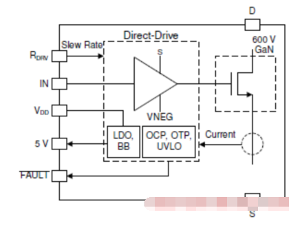
图. LMG341xR070简化框图
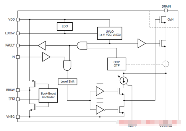
图. LMG341xR070功能框图
参考设计TIDM-02008/TIDM-1007
Bidirectional Interleaved CCM Totem Pole Bridgeless PFC Reference Design Using C2000™ MCU
This reference design illustrates a method to control a bidirectional interleaved continuous conduction mode (CCM) totem pole (TTPL) bridgeless power factor correction (PFC) power stage using a C2000™ microcontroller (MCU) and LMG3410R070. This power
topology is capable of bidirectional power flow (PFC and grid-tied inverter) and it uses Gallium Nitride (GaN) devices, which enables higher efficiency and reduction in size of the power supply. The design supports phase shedding and adaptive dead time for efficiency improvements, input cap compensation scheme for improved power factor at light loads, and non-linear voltage loop to reduce voltage spikes under transient in PFC mode. The hardware and software available with this reference design accelerates time to market.
参考设计TIDM-02008主要特性:
• Interleaved, 3.3-kW, Single-Phase, Bidirectional Bridgeless CCM Totem Pole PFC Stage
• 100-kHz Pulse Width Modulation (PWM) Switching
• Programmable Output Voltage, 380-V DC Output Nominal
• Less Than 2% Total Harmonic Distortion (THD)
• Greater Than 98% Peak Efficiency
• powerSUITE™ Support for Easy Adaptation of Design for User Requirement
• Software Frequency Response Analyzer (SFRA) for Quick Measurement of Open Loop Gain
• Soft Starting of PWM for Reduced Zero Current Spike in TTPL PFC
• Software Support for F28004x Using Driver Library
• Same Source Code Maintained When Running Control Loop on C28x or CLA
参考设计TIDM-02008应用:
• Onboard Chargers for Electronic Vehicles (EVs)
• Telecom Rectifier
• Drives, Welding, and Other Industrial
• Energy Storage System (ESS)
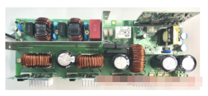
图. 参考设计TIDM-02008外形图
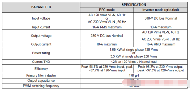
参考设计TIDM-02008主要指标:
责任编辑:David
【免责声明】
1、本文内容、数据、图表等来源于网络引用或其他公开资料,版权归属原作者、原发表出处。若版权所有方对本文的引用持有异议,请联系拍明芯城(marketing@iczoom.com),本方将及时处理。
2、本文的引用仅供读者交流学习使用,不涉及商业目的。
3、本文内容仅代表作者观点,拍明芯城不对内容的准确性、可靠性或完整性提供明示或暗示的保证。读者阅读本文后做出的决定或行为,是基于自主意愿和独立判断做出的,请读者明确相关结果。
4、如需转载本方拥有版权的文章,请联系拍明芯城(marketing@iczoom.com)注明“转载原因”。未经允许私自转载拍明芯城将保留追究其法律责任的权利。
拍明芯城拥有对此声明的最终解释权。


 产品分类
产品分类




 2012- 2022 拍明芯城ICZOOM.com 版权所有 客服热线:400-693-8369 (9:00-18:00)


