


 产品分类
产品分类
TI bq25790 5A四电池开关模式降压-升压电池充电解决方案
 208
208
 拍明
拍明
原标题:TI bq25790 5A四电池开关模式降压-升压电池充电解决方案
TI公司的bq25790是5A一个到四个电池开关模式全集成降压-升压电池充电器,用于锂电池和锂聚合电池, 包括有4个开关的MOSFET(Q1,Q2,Q3和Q4),输入和充电电流检测电路,电池FET(QBAT)和降压-升压转换器所有的回路补偿.器件对充电电池在USB Type-C™和USB供电(USB-PD)应用如智能手机,平板电脑和其它手持设备的全输入电压范围内提供高功率密度和设计灵活性.该器件采用750kHz和1.5MHz可编程开关频率,具有优化的效率:3A ICHG时,2个电池的效率为96.5%(9V输入),15V输入时效率为94.5%.充电电流高达5A,分辨率为10mA,工作电压3.6V到24V, 绝对最大额定值为30V,检查USB BC1.2, SDP, CDP, DCP, HVDCP和非标准适配器,可检查USB BC1.2, SDP, CDP, DCP, HVDCP和非标准适配器. 2个电池时的充电电压调整率为±0.5%高精度,充电电流调整度为±5%,输入电流调整度为±5%,器件具有热调节和热关断特性,输入/电池OVP和OCP,转换器MOSFET OCP以及充电安全计时器.56引脚2.9x3.3mm WCSP封装. 主要用在智能手机,平板电脑和无人机,无线扬声器和数码相机,移动打印机,电子销售终端(EPOS).本文介绍了BQ25790主要特性,功能框图,多种应用框图,以及评估模块BQ25790EVM (bmS027)主要特性,电路图,材料清单和PCB设计图.
The BQ25790 is a fully integrated switch-mode buckboost charger for 1-4 cell Li-ion battery and Lipolymer battery. The integration includes 4 switching MOSFETs (Q1, Q2, Q3, Q4), input and charging current sensing circuits, the battery FET (QBAT) and all the loop compensation of the buck-boost converter. It provides high power density and design
flexibility to charge batteries across the full input voltage range for USB Type-C™ and USB power delivery (USB-PD) applications such as smart phone, tablet and other portable devices.
The charger supports the narrow VDC power path management, in which the system is regulated at a voltage slightly higher than the battery voltage, but not drop below the minimum system voltage. The system keeps operating even when the battery is completely discharged or removed. When load power exceeds input source rating, the battery gets into supplement mode and prevents the input source from being overloaded and the system from crashing.
The device charges a battery from a wide range of the input sources including legacy USB adapter to high voltage USB PD adapter and traditional barrel adapter. The charger automatically sets converter to be buck, boost or buck-boost configurations based on input voltage and battery voltage without the host control. The dual input source selector manages the power flowing from two different input sources. The inputs selection is
controlled by the host through I2C with default source #1 (VAC1) as the primary input and the source #2 (VAC2) as the secondary input.
To support fast charging using adjustable high voltage adapter, the device provides D+/D- handshake. The device is compliant with USB 2.0 and USB 3.0 power delivery specification with input current and voltage regulation. In addition, the Input Current Optimizer (ICO) allows the detection of maximum power point of an unknown input source.
Besides the I2C host controlled charging mode, this charger also supports autonomous charging mode. After power up, the charging is enabled with default register settings. The device can complete a charging cycle without any software engagements. It detects battery voltage and charges the battery in different phases: trickle charging, pre-charging, constant current (CC) charging and constant voltage (CV) charging. At the end of the
charging cycle, the charger automatically terminates when the charge current is below a pre-set limit (termination current) in the constant voltage phase. When the full battery falls below the recharge threshold, the charger will automatically start another charging cycle.
In the absence of input sources, this device supports USB On-the-Go (OTG) function, discharging battery to generate an adjustable 2.8V~22V voltage on VBUS with 10mV step size, which is compliant to the USB PD 3.0 specification defined programmable power supply (PPS) feature.
The charger provides various safety features for battery charging and system operations, including battery temperature negative thermistor monitoring, trickle charge, pre-charge and fast charge timers and overvoltage/over-current protections on battery and input. The thermal regulation reduces charge current when the junction temperature exceeds a programmable threshold. The STAT output of the device reports the charging status and any fault conditions. The PG output indicates if a good power source is present. The INT pin immediately notifies host when fault occurs.
The device also provides a 16-bit analog-to-digital converter (ADC) for monitoring charge current and input/battery/system (VAC, VBUS, BAT, SYS, TS) voltages.
It is available in a 56-pin 2.9mm × 3.3mm WCSP package.
bq25790主要特性:
1• High efficient synchronous Switch Mode buckboost charger for 1-4 cell battery
– 750-kHz and 1.5-MHz Programmable switching frequencies
– Efficiency optimized for charging 2s battery, 96.5% efficiency with 9-V input and 94.5%
efficiency with 15-V input at 3-A ICHG
– Charging current up to 5 A with 10-mA resolution
• Support wide range of input sources
– 3.6-V to 24-V Wide input operating voltage range with 30-V absolute maximum rating
– Maximum power tracking with VINDPM up to 22 V and IINDPM up to 3.3 A
– Detect USB BC1.2, SDP, CDP, DCP, HVDCP and non-standard adapters
• Dual-input power mux controller for source selection
• High level integration
– Four switching MOSFETs and BATFET
– Input current and charging current sensing
• Narrow-VDC (NVDC) Power Path management
• Power USB port from battery (USB OTG)
– 2.8-V to 22-V OTG output voltage with 10-mV resolution to support USB-PD PPS
– OTG Output current regulation up to 3.32 A with 40-mA resolution
• Flexible autonomous and I2C mode for optimal system performance
• Integrated 16-bit ADC for voltage, current and temperature monitor
• Low battery quiescent current
– Typical 21-μA at battery only operation
– Typical 600 nA in Charger Shutdown Mode
• High accuracy
– ±0.5% Charge voltage regulation for 2s battery
– ±5% Charge current regulation
– ±5% Input current regulation
• Safety
– Thermal regulation and thermal shutdown
– Input/battery OVP and OCP
– Converter MOSFETs OCP
– Charging safety timer
• Package
– 56-Pin 2.9mm × 3.3mm WCSP
bq25790应用:
• Smartphone, Tablet, Drone
• Wireless speaker, Digital Camera
• Mobile printer, Electronic point of sales (EPOS)
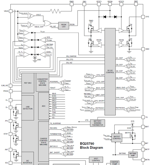
图1. bq25790功能框图

图2. bq25790 OTG模式简化应用框图

图3. bq25790简化电路框图

图4. bq25790两输入源和可选FET应用框图

图5. bq25790单输入源和无可选FET应用框图
评估模块BQ25790EVM (BMS027)
This users guide describes the characteristics, operation, and functionality of the BQ25790 Evaluation Module (EVM). It also describes the equipment, test setup, and software required to operate the EVM. A complete schematic diagram, printed-circuit board (PCB) layouts, and bill of materials (BOM) are also included in this document.
Throughout this users guide, the abbreviations and terms EVM, BQ25790EVM, BMS027, and evaluation module are synonymous with the BQ25790 EVM.
评估模块BQ25790EVM (BMS027)主要特性:
The BQ25790EVM is a complete module for evaluating the BQ25790 in the (WCSP) DSBGA package.
Key features of this EVM include:
• Synchronous Switch Mode Buck-Boost Charger for 1s-4s Battery Configuration for 5-A Charging with 10-mA Resolution
• Support for 3.6-V to 24-V Wide Range of Input Sources USB Auto-Detect, USB PD and Wireless Input
• Dual Input Source Selector to Drive Bi-Directional Blocking NFETs
• Power up USB Port from Battery (USB OTG) with 2.8-V to 22-V OTG Output Voltage with 10-mV Resolution
• Low Battery Quiescent Current < 1 μA in Shutdown Mode

图6. 评估模块BQ25790EVM (BMS027)测试建立图
责任编辑:David
【免责声明】
1、本文内容、数据、图表等来源于网络引用或其他公开资料,版权归属原作者、原发表出处。若版权所有方对本文的引用持有异议,请联系拍明芯城(marketing@iczoom.com),本方将及时处理。
2、本文的引用仅供读者交流学习使用,不涉及商业目的。
3、本文内容仅代表作者观点,拍明芯城不对内容的准确性、可靠性或完整性提供明示或暗示的保证。读者阅读本文后做出的决定或行为,是基于自主意愿和独立判断做出的,请读者明确相关结果。
4、如需转载本方拥有版权的文章,请联系拍明芯城(marketing@iczoom.com)注明“转载原因”。未经允许私自转载拍明芯城将保留追究其法律责任的权利。
拍明芯城拥有对此声明的最终解释权。
相关资讯
:
基于MC33771主控芯片的新能源锂电池管理系统解决方案

AMIC110 32位Sitara ARM MCU开发方案

基于AMIC110多协议可编程工业通信处理器的32位Sitara ARM MCU开发方案

基于展讯SC9820超低成本LTE芯片平台的儿童智能手表解决方案

基于TI公司的AM437x双照相机参考设计

基于MTK6580芯片的W2智能手表解决方案


 2012- 2022 拍明芯城ICZOOM.com 版权所有 客服热线:400-693-8369 (9:00-18:00)


