Cypress CY8C62x5 PSoC 6 MCU IoT开发方案
 177
177
 拍明
拍明
原标题:Cypress CY8C62x5 PSoC 6 MCU IoT开发方案
Cypress公司的CY8C62x5是高性能超低功耗和安全PSoC® 6 MCU平台,组合了双CPU微控制器和具有低功耗闪存技术,数字可编逻辑,高性能模拟/数字转换以及标准通信和计时外设.器件的32位双CPU子系统包括150MHz Arm® Cortex®-M4F (CM4) CPU和单周期乘法器,浮点和存储器保护单元(MPU),100MHz Cortex-M0+ (CM0+) CPU和单周期乘法器和MPU,用户可选择的核逻辑工作电压在1.1V或0.9V.1.1V核电压时工作CPU电流斜率: Cortex-M4为40 μA/MHz, Cortex-M0+为 20 μA/MHz; 0.9V核电压时工作CPU电流斜率: Cortex-M4为22 μA/MHz, Cortex-M0+为 15 μA/MHz.器件具有三个DMA控制器.存储器子系统包括512KB应用闪存,32KB辅助闪存(AUXflash)和32KB监视闪存(SFlash),支持边写边读(RWW)以及两个8KB闪存缓冲器,每个CPU一个.此外还包括256KB SRAM以及OTP 1Kb eFuse阵列.器件低功耗1.7V-3.6V工作,主要用在物联网(IoT).本文介绍了CY8C62x5系列主要特性,框图和时钟框图, 模拟子系统框图, CapSense硬件子系统图以及PSoC 62S1 Wi-Fi BT先锋板主要特性,框图和引脚图以及板包含元件,电路图和PCB设计图.
PSoC® 6 MCU is a high-performance, ultra-low-power and secure MCU platform, purpose-built for IoT applications. The CY8C62x5 product line, based on the PSoC 6 MCU platform, is a combination of a dual CPU microcontroller with low-power flash technology, digital programmable logic, high-performance analog-to-digital conversion and standard communication and timing peripherals.
CY8C62x5系列主要特性:
32-bit Dual CPU Subsystem
■ 150-MHz Arm® Cortex®-M4F (CM4) CPU with single-cycle multiply, floating point, and memory protection unit (MPU)
■ 100-MHz Cortex-M0+ (CM0+) CPU with single-cycle multiply and MPU
■ User-selectable core logic operation at either 1.1 V or 0.9 V
■ Active CPU current slope with 1.1-V core operation
❐ Cortex-M4: 40 μA/MHz
❐ Cortex-M0+: 20 μA/MHz
■ Active CPU current slope with 0.9-V core operation
❐ Cortex-M4: 22 μA/MHz
❐ Cortex-M0+: 15 μA/MHz
■ Three DMA controllers
Memory Subsystem
■ 512-KB application flash, 32-KB auxiliary flash (AUXflash), and 32-KB supervisory flash (SFlash); read-while-write (RWW) support. Two 8-KB flash caches, one for each CPU.
■ 256-KB SRAM with programmable power control and retention granularity
■ One-time-programmable (OTP) 1-Kb eFuse array
Low-Power 1.7-V to 3.6-V Operation
■ Six power modes for fine-grained power management
■ Deep Sleep mode current of 7 μA with 64-KB SRAM retention
■ On-chip DC-DC buck converter, <1 μA quiescent current
■ Backup domain with 64 bytes of memory and real-time clock
Flexible Clocking Options
■ On-chip crystal oscillators (16 to 35 MHz, and 32 kHz)
■ Phase-locked loop (PLL) for multiplying clock frequencies
■ 8-MHz internal main oscillator (IMO) with ±2% accuracy
■ Ultra-low-power 32-kHz internal low-speed oscillator (ILO)
■ frequency-locked loop (FLL) for multiplying IMO frequency
Quad-SPI (QSPI)/Serial Memory Interface (SMIF)
■ Execute-In-Place (XIP) from external quad SPI flash
■ On-the-fly encryption and decryption
■ 4-KB cache for greater XIP performance with lower power
■ Supports single, dual, quad, dual-quad, and octal interfaces with throughput up to 640 Mbps
Segment LCD Drive
■ Supports up to 63 segments and up to 8 commons.
■ Operates in system Deep Sleep mode
Serial Communication
■ Seven run-time configurable serial communication blocks (SCBs)
❐ Six SCBs: configurable as SPI, I2C, or UART
❐ One Deep Sleep SCB: configurable as SPI or I2C
■ USB Full-Speed device interface
■ One SD Host Controller/eMMC/SD controller
■ One CAN FD block
Timing and Pulse-Width Modulation
■ Twelve timer/counter/pulse-width modulators (TCPWMs)
■ Center-aligned, edge, and pseudo-random modes
■ Comparator-based triggering of Kill signals
Programmable Analog
■ 12-bit 2-Msps SAR ADC with differential and single-ended modes and 16-channel sequencer with result averaging
■ Two low-power comparators available in system Deep Sleep and Hibernate modes
■ Built-in temperature sensor connected to ADC
Up to 64 Programmable GPIOs
■ Two Smart I/O™ ports (8 I/Os) enable Boolean operations on
GPIO pins; available during system Deep Sleep
■ Programmable drive modes, strengths, and slew rates
■ Two overvoltage-tolerant (OVT) pins
Capacitive Sensing
■ Cypress CapSense® sigma-delta (CSD) provides best-in-class signal-to-noise ratio (SNR), liquid tolerance, and proximity sensing
■ Enables dynamic usage of both self and mutual sensing
■ Automatic hardware tuning (SmartSense™)
Security Built into Platform Architecture
■ ROM-based root of trust via uninterruptible Secure Boot
■ Authentication during boot using hardware hashing
■ Step-wise authentication of execution images
■ Secure execution of code in execute-only mode for protected routines
■ All debug and test ingress paths can be disabled
■ Up to eight protection contexts
Cryptography Accelerator
■ Hardware acceleration for symmetric and asymmetric cryptographic methods and hash functions
■ True random number generation (TRNG) function
Packages
■ 100 TQFP, 68 QFN, 49 WLCSP
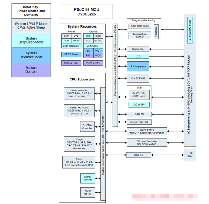
图1. CY8C62x5系列框图
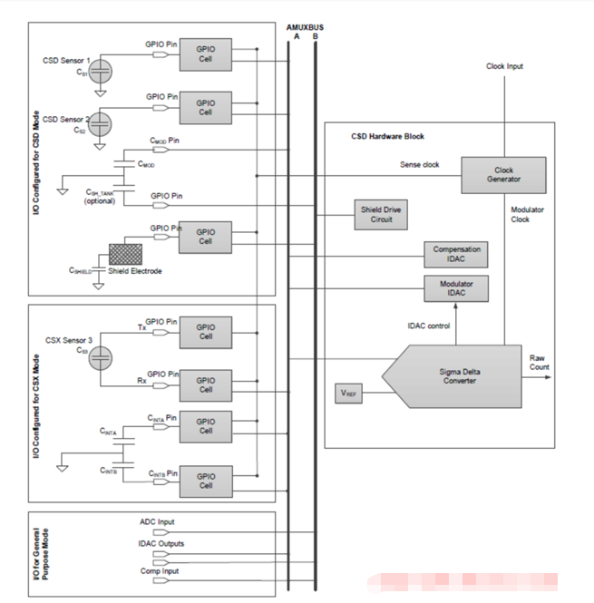
图4. CapSense硬件子系统图
评估板CYW9P62S1-43438EVB-01 PSoC 62S1 Wi-Fi BT先锋套件
Thank you for your interest in the CYW9P62S1-43438EVB-01 PSoC 62S1 Wi-Fi BT Pioneer Kit. The PSoC 62S1 Wi-Fi BT Pioneer Kit enables you to evaluate and develop your applications using the PSoC 62 Series MCU (hereafter called “PSoC 6 MCU”) and CYW43438 Wi-Fi/BT combo device.
PSoC 6 MCU is Cypress latest, ultra-low-power PSoC specifically designed for wearables and IoT products. PSoC 6 MCU is a true programmable embedded system-on-chip, integrating a 150-MHz Arm® Cortex®-M4 as the primary application processor, a 100-MHz Arm Cortex-M0+ that supports low-power operations, up to 2 MB Flash and 1 MB SRAM, CapSense® touch-sensing, and programmable analog and digital peripherals that allow higher flexibility, in-field tuning of the design, and faster time-to-market. The PSoC 6 MCU on this kit, CY8C6247BZI-D54 has 1 MB Flash and 288 KB SRAM.
The PSoC 62S1 Wi-Fi BT Pioneer Board offers compatibility with Arduino™ shields. The board features a PSoC 6 MCU, and a CYW43438 Wi-Fi/Bluetooth combo module. Cypress CYW43438 is a highly integrated single-chip solution and offers the lowest BOM in the industry for smartphones, tablets, and a wide range of other portable devices. The chip includes a 2.4 GHz WLAN IEEE 802.11 b/g/n MAC/baseband/radio, and Bluetooth 4.2. The WLAN section supports SDIO interface to the host MCU (PSoC 6 MCU), and the Bluetooth section supports high-speed 4-wire UART interface to the host MCU. In addition, the board features an onboard programmer/debugger (KitProg3), a 512-Mbit Quad SPI NOR flash, a 4-Mbit Quad SPI F-RAM, a micro-B connector for USB device interface,a 5-segment CapSense slider, two CapSense buttons, an RGB LED, two user LEDs, one
potentiometer, and two push buttons.
You can use ModusToolbox™ to develop and debug your PSoC 6 MCU projects. ModusToolbox software is a set of tools that enable you to integrate Cypress devices into your existing development methodology.
If you are new to PSoC 6 MCU and ModusToolbox IDE, refer to the application note AN228571 -Getting Started with PSoC 6 MCU on ModusToolbox to help you familiarize with the PSoC 6 MCU and help you create your own design using the ModusToolbox IDE.
Kit Contents
The CYW9P62S1-43438EVB-01 PSoC 62S1 Wi-Fi BT Pioneer Kit has the following contents.
■ PSoC 62S1 Wi-Fi BT Pioneer Board
■ USB Type-A to Micro-B cable
■ Four jumper wires (4 inches each)
■ Two jumper wires (5 inches each)
■ Quick Start Guide
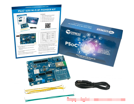
图5.评估板CYW9P62S1-43438EVB-01 PSoC 62S1 Wi-Fi BT先锋套件外形图
PSoC 62S1 Wi-Fi BT先锋板主要特性:
■ CYW9P62S1-43438CAR-01 carrier module that contains AW-CU427-01H System in Package (SiP) module by AzureWave, which has
❐ PSoC 6 MCU (CY8C6247BZI-D54)
❐ CYW43438KUBG, 2.4 GHz WLAN and Bluetooth 4.2 compliant device supporting Dual-mode Bluetooth Classic and Bluetooth Low Energy (BT and BLE) operation
■ 512-Mbit external Quad SPI NOR Flash that provides a fast, expandable memory for data and code
■ 4-Mbit Quad SPI ferroelectric random-access memory (F-RAM)
■ KitProg3 onboard SWD programmer/debugger with USB-UART and USB-I2C bridge functionality
■ CapSense touch-sensing slider (5 elements), two buttons, based on self-capacitance (CSD) and mutual-capacitance (CSX) sensing
■ A micro-B connector for USB device interface for PSoC 6 MCU
■ 3.3 V operation of PSoC 6 MCU is supported
■ Two user LEDs, an RGB LED, two user buttons, and a reset button for the PSoC 6 MCU
■ A potentiometer
■ One Mode selection button and one Status LED for KitProg3
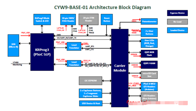
图6.评估板CYW9P62S1-43438EVB-01先锋套件框图
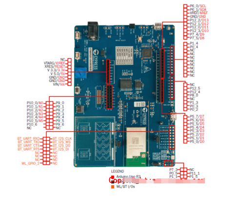
图6.PSoC 62S1 Wi-Fi BT先锋板引脚图
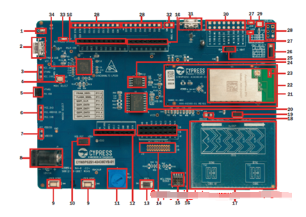
图7.PSoC 62S1 Wi-Fi BT先锋板外形图:顶视图
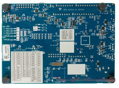
图8.PSoC 62S1 Wi-Fi BT先锋板外形图:底视图
PSoC 62S1 Wi-Fi BT先锋板包含下列元件:
1. Power LED (LED1): This Yellow LED indicates the status of power supplied to board.
2. KitProg3 USB connector (J6): The USB cable provided along with the PSoC 62S1 Wi-Fi BT Pioneer Board connects between this USB connector and the PC to use the KitProg3 onboard programmer and debugger and to provide power to the board.
3. PSoC 6 MCU VDD power selection jumper (J14): This jumper is used to select the PSoC 6 MCU VDD supply voltage between 1.8 V and 3.3 V. J14 is not loaded for this kit and R83 is loaded, due to which only 3.3 V operation is supported.
4. KitProg3 programming mode selection button (SW3): This button can be used to switch between various modes of operation of KitProg3 (CMSIS-DAP BULK, CMSIS-DAP HID or DAPLink modes). For more details, see the KitProg3 User Guide.
5. PSoC 6 MCU VDD current measurement jumper (J15): An ammeter can be connected to this jumper to measure the current consumed by the PSoC 6 MCU VDD power domain. Please refer to Power Supply System on page 33 for details on power domains that are monitored by current measurement jumpers.
6. PSoC 6 MCU VDDIO2 and CYW43438 VDDIO power selection jumper (J16): This jumper is used to select the PSoC 6 MCU VDDIO2 and CYW43438 VDDIO supply voltage between 1.8 V and 3.3 V. This is not loaded by default. This board supports operation of VDDIO at 1.8 V.
7. PSoC 6 MCU VDDIO0 current measurement jumper (J19): An ammeter can be connected to this jumper to measure the current consumed by the PSoC 6 MCU VDDIO0 power domain. This is not loaded by default. Before populating the jumper for making current measurements, ensure that R97 is removed.
8. External power supply VIN connector (J5): This connector connects an external DC power supply input to the onboard regulators.
9. PSoC 6 MCU user buttons (SW2 and SW4): These buttons can be used to provide an input to the PSoC 6 MCU. Note that by default these buttons connect the PSoC 6 MCU pin to ground when pressed, so you need to configure the PSoC 6 MCU pin as a digital input with resistive pullup for detecting the button press. These buttons also provide a wake-up source from low-power modes of the device.
10. Potentiometer connection jumper (J25): This jumper connects the PSoC 6 MCU VDDA to the potentiometer.
11. Potentiometer (R1): This is a 10K Ω potentiometer connected to PSoC 6 MCU pin P10[6]. It can be used to simulate a sensor output to the PSoC 6 MCU.
12. Arduino-compatible power header (J1): This header powers the Arduino shields. It also has a provision to power the kit though the VIN input.
13. PSoC 6 MCU reset button (SW1): This button is used to reset the PSoC 6 MCU. It connects the PSoC 6 MCU reset (XRES) pin to ground.
14. PSoC 6 MCU debug and trace header (J12): This header can be connected to an Embedded Trace Macrocell (ETM)-compatible programmer/debugger. This is not loaded by default.
15. PSoC 6 MCU program and debug header (J11): This 10-pin header allows you to program and debug the PSoC 6 MCU using an external programmer such as MiniProg4.
16. Arduino Uno R3-compatible I/O headers (J2, J3, and J4): These I/O headers bring out pins from the PSoC 6 MCU to interface with Arduino shields. Some of these pins are multiplexed with onboard peripherals and are not connected to the PSoC 6 MCU by default. For a detailed information on how to rework the kit to access these pins, see Table 2-1 on page 13.
17. CapSense slider (SLIDER) and buttons (BTN0 and BTN1): The CapSense touch-sensing slider and two buttons, all of which are capable of both self-capacitance (CSD) and mutualcapacitance (CSX) operation, allow you to evaluate Cypress fourth-generation CapSense technology.
The slider and buttons have a 1-mm acrylic overlay for smooth touch sensing.
18. PSoC 6 MCU VDDIO2 current measurement jumper (J18): An ammeter can be connected to this jumper to measure the current consumed by the PSoC 6 MCU VDDIO2 power domain. This jumper is not loaded by default on the board. Before populating the jumper for current measurements, ensure that R94 is removed.
19. CYW43438 VDDIO current measurement jumper(J17): An ammeter can be connected to this jumper to measure the current consumed by the CYW43438 VDDIO power domain.
20. Cypress serial NOR flash memory (S25FL512S, U3): A S25HL512S NOR flash of 512-Mbit capacity is connected to the Quad SPI interface of the PSoC 6 MCU. The NOR device can be used for both data and code memory with execute-in-place (XIP) support and encryption.
21. AzureWave AW-CU427-01H SiP module: AW-CU427-01H is an SiP module that contains the PSoC 6 MCU (CY8C6247BZI-D54) and the CYW43438 (Wi-Fi + Bluetooth combo device). The CYW43438 includes a 2.4 GHz WLAN IEEE 802.11 b/g/n MAC/baseband/radio, and Bluetooth
4.2. In addition, it integrates a power amplifier (PA) that meets the output power requirements of most handheld systems, a low-noise amplifier (LNA) for best-in-class receiver sensitivity, and an internal transmit/receive (iTR) RF switch, further reducing the overall solution cost and printed circuit board area.
22. Cypress PSoC 6 (1M) with CYW43438 AzureWave PCB MOD Carrier Module
(CYW9P62S1-43438CAR-01, MOD1): This kit is designed to highlight the features of the
PSoC 6 MCU on the CYW9P62S1-43438CAR-01. For details, see CYW9P62S1-43438CAR-01 (MOD1) on page 27. This kit is designed to highlight the features of the PSoC 6 MCU. For details on PSoC 6 MCU pin mapping, refer to Table 2-1 on page 13.
23. Wi-Fi/BT antenna: This is an onboard antenna connected to the Wi-Fi and Bluetooth module.
24. Cypress Quad SPI Ferroelectric-RAM (CY15B104QSN, U4): The CY15B104QSN is a 4-Mbit nonvolatile memory employing an advanced ferroelectric process. F-RAM is nonvolatile and performs reads and writes similar to a RAM. It provides reliable data retention for 151 years and is connected to the Quad SPI interface of the PSoC 6 MCU.
25. CYW43438 VBAT current measurement jumper (J8): An ammeter can be connected to this jumper to measure the current consumed by the CYW43438 VBAT power domain.
26. CYW43438 VBAT power selection jumper (J9): This jumper is used to select the CYW43438 VBAT supply voltage between 1.8 V, 3.3 V and 3.6 V. This board supports VBAT voltages of 3.3 V and 3.6 V. VBAT is 3.3 V when the jumper is not inserted and 3.6 V when the jumper is inserted.
27. PSoC 6 MCU user LEDs (LED8 and LED9): These two user LEDs can operate at the entire operating voltage range of the PSoC 6 MCU. The LEDs are active LOW, so the pins must be driven to logic LOW to turn ON the LEDs.
28. PSoC 6 I/O header (J21, J22, J24): These headers provide connectivity to PSoC 6 MCU GPIOs that are not connected to the Arduino compatible headers. Some of these I/Os are also connected to on-board peripherals see Table 2-1 on page 13 for pin mapping.
29. RGB LED (LED5): This onboard RGB LED can be controlled by the PSoC 6 MCU. The LEDs are active LOW, so the pins must be driven to ground to turn ON the LEDs.
30. Wi-Fi/BT GPIO header (J23): This header brings out a few IOs of the CYW43438 for general purpose applications.
31. PSoC 6 USB device connector (J7): The USB cable provided with the PSoC 62S1 Wi-Fi BT Pioneer Kit can also be connected between this USB connector and the PC to use the PSoC 6 MCU USB device applications.
32. Optional USB Host power supply header (J10): This header provides an option to supply external power to the PSoC 6 USB when used as a USB Host. This is not loaded by default.
33. KitProg3 status LED (LED2): This Yellow LED indicates the status of KitProg3. For details on the KitProg3 status, see the KitProg3 User Guide.
34. KitProg3 (PSoC 5LP) programmer and debugger (CY8C5868LTI-LP039, U2): The PSoC 5LP device (CY8C5868LTI-LP039) serving as KitProg3, is a multi-functional system, which includes a SWD programmer, debugger, USB-I2C bridge and USB-UART bridge. For more details, see the KitProg3 User Guide.
责任编辑:David
【免责声明】
1、本文内容、数据、图表等来源于网络引用或其他公开资料,版权归属原作者、原发表出处。若版权所有方对本文的引用持有异议,请联系拍明芯城(marketing@iczoom.com),本方将及时处理。
2、本文的引用仅供读者交流学习使用,不涉及商业目的。
3、本文内容仅代表作者观点,拍明芯城不对内容的准确性、可靠性或完整性提供明示或暗示的保证。读者阅读本文后做出的决定或行为,是基于自主意愿和独立判断做出的,请读者明确相关结果。
4、如需转载本方拥有版权的文章,请联系拍明芯城(marketing@iczoom.com)注明“转载原因”。未经允许私自转载拍明芯城将保留追究其法律责任的权利。
拍明芯城拥有对此声明的最终解释权。


 产品分类
产品分类




 2012- 2022 拍明芯城ICZOOM.com 版权所有 客服热线:400-693-8369 (9:00-18:00)


