基于C8051F9XX系列的超低功耗单片机的脉搏血氧仪解决方案
 423
423
 拍明
拍明
应用领域:医疗健康
方案类型:原型方案
主控芯片:C8051F912
方案概述
脉搏血氧仪以无创方式通过手指检测人体的血氧饱和度。同时还可以检测动脉脉动,因此也可以计算心率,是测量人体动脉血液中氧气含量的一种医疗设备,适用于家庭、医院、社区医疗、运动保健等范围。脉搏血氧仪具有体积小、功耗低、便携、操作方便等特点。
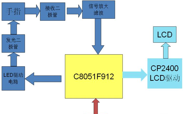
C8051F9XX
1. Introduction
The C8051F9xx family of low-voltage/low-power MCUs is an excellent choice for battery-powered embedded
systems. Following are some of the key features of this product family:
Low Active and Inactive Mode Current
150 µA/MHz, 160 µA/MHz, or 170 µA/MHz Active Mode Current @ 25 MHz
< 1 µA Sleep Mode Current
Fast Wakeup Time and Fast Code Execution
400 ns Suspend Mode Wakeup (using the low power internal oscillator)
2 µs Sleep Mode Wakeup (two-cell mode) or
10 µs Sleep Mode Wakeup (one-cell mode)
Up to 25 MIPs Operation
Fast ADC Acquisition Time
1.5 µs VREF turn-on time, occurs while ADC is tracking
3.3 µs back-to-back analog acquisition time
Support for 1 and 2 Cell Battery Configurations
0.9–1.8 V supply voltage range allows the system to be powered from a single alkaline or silver oxide battery.
1.8–3.6 V supply voltage range allows the system to be powered from a single lithium battery or two alkaline batteriesplaced in series.The C8051F9xx MCU family is very flexible and provides application software control over many factors affectingdevice power consumption. This application note describes how to achieve maximum efficiency in each powermode and how to optimize application code to take advantage of the low power features of the C8051F9xx family.Included with this application note is example software that can be used to place the C8051F9xx MCU into each ofits power modes for supply current measurements. Also included is a low-power software template that may beused as a starting point for new code development. The software can be found in the AN358SW.zip archive, whichis distributed with this application note.
2. Key Points
Two Regions of Operation—C8051F9xx devices have two distinct regions of operation. The Flash one-shotcircuit must be disabled (bypassed) for high system clocks and enabled for system clocks in order to minimizesupply current in the normal power mode. The optimumcrossover frequency is 10 MHz (C8051F93x/2x) or 14MHz (C8051F91x/0x/9x/8x).
Sleep Mode Supply Current—The current in Sleep mode should always be < 1 µA at room temperature, evenwhen the SmaRTClock is running. If the current meter is measuring a current higher than 1 uA, then the deviceis not configured properly; one or more GPIO pins are sourcing current to an external circuit, or a high-speedsignal is being applied to a port pin (e.g., an external CMOS clock).
Software Considerations—The proper entry and exit procedures should be used when entering and exiting alow-power mode. This ensures that the device will work in a reliable and predictable manner.
SmaRTClock Alarm Events—The SmaRTClock ALRM flag is not persistent and is automatically cleared byhardware after 1 SmaRTClock cycle. The RTCAWK flag in the PMU0CF register is persistent and can be usedto detect a SmaRTClock alarm event after the ALRM flag has been cleared.
Flash Memory Operations—If erasing Flash memory, be sure to set the SmaRTClock alarm interval to a valuelonger than 36 ms to ensure that an alarm is not missed. When writing Flash memory, ensure that the alarminterval is longer than 71 µs.
Measuring Current—The software supplied with this application note allows the digital supply currentspecification in the data sheet to be achieved. Any current flowing through the GPIO pins is in addition to thedigital supply current required to operate the device. For example, driving a 24.5 MHz clock signal on a GPIOpin with a 3.3 V supply voltage can increase the supply current by 3 mA.
3. Power Modes Overview
The C8051F9xx family of MCUs support five power modes: Normal, Idle, Stop, Suspend and Sleep. A summary ofthe power modes can be found in Table 1. Detailed descriptions of each mode can be found in the PowerManagement chapter of the device data sheet.Normal and Idle modes are classified as Active Power Modes because the system clock is active and powerconsumption scales with the clock frequency. Typical supply currents for each of the three different system clocksources (24.5 MHz Precision Oscillator, 20 MHz Low Power Oscillator, and 32.768 kHz SmaRTClock Oscillator)are provided in Table 1. Stop, Suspend, and Sleep modes are classified as Inactive Power Modes because thesystem clock is stopped.
Since the system clock in most low-power applications is not always present, the C8051F9xx MCUs have an ultralow-powerSmaRTClock that can be used for timekeeping. The SmaRTClock oscillator requires less than 1 uA ofsupply current and can remain functional even when the MCU goes into its lowest power Sleep mode.

4. Minimizing Active Mode Current
The active modes in a low-power system typically require the most supply current; however, they are the modes inwhich the most critical system tasks are completed. Minimizing Active mode time is one of the best power savingstrategies. This can be achieved by operating at the fastest possible system clock frequency. Since the MCU ismost efficient at fast system clocks, minimizing active mode time results in greater overall benefit than reducingpeak current.
The following figures show the typical supply current in Normal and Idle modes as a function of the system clockfrequency. There are two observations to note about the Normal mode curves: 1) at the crossover point, the slopeof the supply current vs. frequency curve changes. This divides the curve into two piece wise linear regions. 2) Theabsolute current per MHz decreases as the system clock frequency increases. At low frequencies, the CPUoperates at a higher µA/MHz. As frequency increases, the µA/MHz drops and can be less than 150 µA/MHz onsome devices.The Active supply current can be influenced by a number of factors including supply voltage, temperature, systemclock frequency, power mode, and other factors under the control of application software.
4.1. Effect of Supply Voltage
In most CMOS circuits, supply voltage has the greatest effect on supply current. However, since the C8051F9xxMCUs have an on-chip LDO for regulating the voltage supplied to the digital circuitry, supply voltage has a minimaleffect on supply current. In fact, the supply current variation over the entire input voltage range (1.8–3.6 V) istypically less than ±10 µA from the midpoint voltage of 2.7 V.
4.2. Effect of Temperature
Changes in temperature can affect the active supply current. As temperatures rise, the supply current alsoincreases, and as temperatures drop, the supply current decreases. The supply current variation over the entireoperating temperature range (–40 to +85 °C) is typically less than ±5% from the supply current measured at 25 °C.
4.3. Effect of System Clock Frequency
The system clock frequency has the most significant effect on the active supply current. As the clock frequencyincreases, supply current and power efficiency increase, as shown in the following figures. When executing a taskthat requires a fixed number of instructions, the system clock should be set as fast as possible. The limiting factorin increasing the system clock should be the ability of the power supply to handle the increased peak currents.For tasks that require a fixed amount of time to complete (e.g., waiting for a UART byte to be clocked in),
increasing the system clock actually decreases power efficiency because the peak current increases while noadditional work is being completed. In these situations, the system clock frequency should be minimized and the
CPU placed in Idle mode.
4.4. Effect of Power Mode
The C8051F9xx MCUs have two Active Power Modes in which the system clock is running. Normal mode powerconsumption is shown in Figure 1, Figure 3, and Figure 5, and Idle mode power consumption is shown in Figure 4,Figure 6, and Figure 6. As a rule of thumb, placing the CPU in Idle mode will typically reduce the supply current byapproximately 50%.
4.5. Optimizing Application Software
To achieve the supply current measurements listed in this application note and in the device data sheet, applicationsoftware must properly configure the device into its optimum power setting. These low-power optimizations forActive Power Modes are as follows:
1. For system clock frequencies greater than the crossover frequency, disable (bypass) the one-shot circuit bysetting the BYPASS bit (FLSCL.6) to logic 1. For system clock frequencies less than the crossover frequency,enable the one-shot circuit by clearing the BYPASS bit (FLSCL.6) to logic 0 and immediately following thisoperation with a write of a non-zero value to the FLWR register (only required for C8051F93x/2x devices). Adetailed description of the one-shot circuit can be found in the Flash chapter of the device data sheet. Leavingthe one-shot enabled for frequencies higher than the crossover frequency can result in 40% higher supplycurrent. Leaving the one-shot bypassed for frequencies less than crossover frequency can result in greater than500% increase in supply current.Note: The optimum one-shot crossover frequency is 14 MHz on C8051F91x/0x/9x/8x devices and 10 MHz on
2. If the Low Power Oscillator is not selected as the system clock source, clear all wake-up source flags by writing0x20 to the PMU0CF register. Always use direct writes or reads when accessing this register. Clearing thewake-up source flags allows the Low Power Oscillator to be automatically disabled by hardware when it is notneeded. This optimization reduces the supply current by 100 uA.
3. If the Precision Oscillator is not selected as the system clock source, disable the Precision Oscillator Bias byclearing the OSCBIAS bit (REG0CN.4) to logic 0. This optimization reduces the supply current by 85 uA.
4. When using one of the internal oscillators as the system clock source, disable the missing clock detector resetsource in the RSTSRC register. Always use direct writes or reads when accessing this register and be carefulnot to disable the VDD Monitor as a reset source. This optimization reduces the supply current by 10 uA.
5. Disable the 1.8 V supply monitor in systems that use an external supply monitor or when a proper supplyvoltage is guaranteed (e.g., a system that uses a permanent battery where behavior at battery end-of-life is adon’t care). This optimization reduces the supply current by 5 to 20 uA depending on supply voltage.
6. Whenever possible, try to execute code at the fastest possible clock frequency and use Idle mode to pausecode execution when waiting for a specific event to occur (e.g., timer overflow flag in a software delay loop,GPIO pin changing state, UART transmission or ADC conversion to complete, etc.).
7. If software contains small loops, such as a while(1) statement, ensure that the loop does not straddle a flashrow boundary. Devices with 1024 byte Flash pages have a row boundary of 128 bytes, and devices with 512byte Flash pages have a row boundary of 64 bytes. Supply current can increase by up to 30% when a shortloop straddles a Flash row boundary. See the Flash chapter of the MCU data sheet for more details aboutminimizing Flash read current.
C8051F9XX产品系列:
C8051F930, C8051F931, C8051F920, C8051F921, C8051F912, C8051F911, C8051F902, C8051F901,C8051F990, C8051F991, C8051F996, C8051F997, C8051F980, C8051F981, C8051F982, C8051F983,C8051F985, C8051F986, C8051F987, C8051F988, C8051F989
脉搏血氧仪
脉搏血氧仪提供了以无创方式测量血氧饱和度或动脉血红蛋白饱和度的方法。脉搏血氧仪还可以检测动脉脉动,因此也可以计算并告知病人的心率。脉搏血氧仪是测量病人动脉血液中氧气含量的一种医疗设备。
测量原理
基于动脉搏动期间光吸收量的变化。分别位于可见红光光谱(660纳米)和红外光谱(940纳米)的两个光源交替照射被测试区(一般为指尖或耳垂)。在这些脉动期间所吸收的光量与血液中的氧含量有关。微处理器计算所吸收的这两种光谱的比率,并将结果与存在存储器里的饱和度数值表进行比较,从而得出血氧饱和度。
典型的血氧仪传感器有一对LED,它们通过病人身体的半透明部位(通常是指尖或耳垂)正对着一个光电二极管。其中一个LED是红光的,波长为660nm;另一个是红外线的,波长是940nm。血氧的百分比是根据测量这两个具有不同吸收率的波长的光通过身体后计算出的。
适用人群
病人在急救和转运过程中、消防抢险、高空飞行必须监测血氧;心脏病、高血压、糖尿病人,特别是老人都会有呼吸方面的问题,监测血氧指标可很好地了解自己的呼吸、免疫系统是否正常,血氧饱和度已成为普通家庭日常监测的重要生理指标;医护人员在查房和出诊是也将血氧作为必监测项目,使用数量有压过听诊器的趋势;呼吸疾病患者特别是长期打鼾的、使用呼吸机和制氧机的患者,在日常生活中使用血氧仪来监测治疗效果;户外运动者、登山爱好者、体育运动者在运动时都使用血氧仪,及时知道自己的身体情况,并采取必要的保护措施。
主要组件
一个微处理器、存储器(EPROM与RAM)、两个控制LED的数模转换器、对光电二极管接收的信号进行滤波与放大的器件、将接收信号数字化以提供给微处理器的模数转换器。LED与光电二极管放置在与患者指尖或耳垂接触的小型探针中。脉搏血氧仪一般还包括小型液晶显示器。
责任编辑:Davia
【免责声明】
1、本文内容、数据、图表等来源于网络引用或其他公开资料,版权归属原作者、原发表出处。若版权所有方对本文的引用持有异议,请联系拍明芯城(marketing@iczoom.com),本方将及时处理。
2、本文的引用仅供读者交流学习使用,不涉及商业目的。
3、本文内容仅代表作者观点,拍明芯城不对内容的准确性、可靠性或完整性提供明示或暗示的保证。读者阅读本文后做出的决定或行为,是基于自主意愿和独立判断做出的,请读者明确相关结果。
4、如需转载本方拥有版权的文章,请联系拍明芯城(marketing@iczoom.com)注明“转载原因”。未经允许私自转载拍明芯城将保留追究其法律责任的权利。
拍明芯城拥有对此声明的最终解释权。


 产品分类
产品分类




 2012- 2022 拍明芯城ICZOOM.com 版权所有 客服热线:400-693-8369 (9:00-18:00)


