Renesas RA6M2 High-Performance ARM MCU IoT Development Solution
 113
113
 拍明
拍明
原标题:Renesas RA6M2 High-Performance ARM MCU IoT Development Solution
Renesas' RA6M2 series is a high-performance Arm® Cortex®-M4 core microcontroller (mcu) that provides a single DMA Ethernet MAC to ensure high data throughput. It is manufactured using an efficient 40nm process, supporting open source and flexibility Ecosystem concept (Flexible Software Package (FSP) based on FreeRTOS), and can be extended to use other RTOS and middleware. The MCU integrates multiple software and pin-compatible Arm® 32-bit cores, sharing the basic set of Renesas peripherals. It is convenient for design upgrade and product development based on an effective platform. The operating frequency of the MCU core is up to 120MHz, 1MB of code flash and 384kB SRAM. Its floating-point unit (FPU) has an Armv7E-M architecture with a DSP instruction set and supports 4GB addresses Space, on-chip debugging system has JTAG, SWD and ETM, boundary scan and ARM memory protection unit (ARM MPU). The connectivity of the device includes Ethernet MAC controller (ETHERC), Ethernet DMA controller (EDMAC) and USB 2.0 full speed (USBFS) module. China Power Grid organizes the following detailed information for you, mainly used in wired Ethernet, security system (fire detection, burglar detection and panel control), measurement (electric meter, automatic meter reading), industry (robot, door opener) , Sewing machine, vending machine and UPS) as well as HVAC (heating, air conditioning, boiler control) and general. This article introduces the main features of RA6M2, block diagram and evaluation board EK-RA6M2 v1 main features, block diagram, circuit diagram, bill of materials and PCB design drawings.
The Renesas RA6M2 group of microcontrollers (MCUs) uses the high-performance Arm® Cortex®-M4 core and offers Ethernet MAC with individual DMA, to ensure high data throughput. The RA6M2 is built on a highly efficient 40nm process and is supported by an open and flexible ecosystem concept—the Flexible Software Package (FSP), built on FreeRTOS—and is expandable to use other RTOSes and middleware. The RA6M2 is suitable for IoT applications requiring Ethernet, security, large embedded RAM, and low active power consumption.
The MCU integrates multiple series of software- and pin-compatible Arm®-based 32-bit cores that share a common setof Renesas peripherals to facilitate design scalability and efficient platform-based product development.
The MCU in this series incorporates a high-performance Arm Cortex®-M4 core running up to 120 MHz with thefollowing features:
Up to 1-MB code flash memory
384-KB SRAM
Capacitive Touch Sensing Unit (CTSU)
Ethernet MAC Controller (ETHERC), USBFS, SD/MMC Host Interface
Quad Serial Peripheral Interface (QSPI)
Security and safety features
12-bit A/D Converter (ADC12)
12-bit D/A Converter (DAC12)
Analog peripherals.
Main features of RA6M2:
■ Arm Cortex-M4 Core with Floating Point Unit (FPU)
Armv7E-M architecture with DSP instruction set
Maximum operating frequency: 120 MHz
Support for 4-GB address space
On-chip debugging system: JTAG, SWD, and ETM
Boundary scan and Arm Memory Protection Unit (Arm MPU)
■ Memory
Up to 1-MB code flash memory (40 MHz zero wait states)
32-KB data flash memory (125,000 erase/write cycles)
Up to 384-KB SRAM
Flash Cache (FCACHE)
Memory Protection Units (MPU)
Memory Mirror Function (MMF)
128-bit unique ID
■ Connectivity
Ethernet MAC Controller (ETHERC)
Ethernet DMA Controller (EDMAC)
USB 2.0 Full-Speed (USBFS) module
- On-chip transceiver
Serial Communications Interface (SCI) with FIFO × 10
Serial Peripheral Interface (SPI) × 2
I2C bus interface (IIC) × 3
Controller Area Network (CAN) × 2
Serial Sound Interface Enhanced (SSIE)
SD/MMC Host Interface (SDHI) × 2
Quad Serial Peripheral Interface (QSPI)
IrDA interface
Sampling Rate Converter (SRC)
External address space
- 8-bit or 16-bit bus space is selectable per area
- SDRAM support
■ Analog
12-bit A/D Converter (ADC12) with 3 sample-and-hold circuitseach × 2
12-bit D/A Converter (DAC12) × 2
High-Speed Analog Comparator (ACMPHS) × 6
Temperature Sensor (TSN)
■ Timers
General PWM Timer 32-bit Enhanced High Resolution(GPT32EH) × 4
General PWM Timer 32-bit Enhanced (GPT32E) × 4
General PWM Timer 32-bit (GPT32) × 6
Asynchronous General-Purpose Timer (AGT) × 2
Watchdog Timer (WDT)
■ Safety
Error Correction Code (ECC) in SRAM
SRAM parity error check
Flash area protection
ADC self-diagnosis function
Clock Frequency Accuracy Measurement Circuit (CAC)
Cyclic Redundancy Check (CRC) calculator
Data Operation Circuit (DOC)
Port Output Enable for GPT (POEG)
Independent Watchdog Timer (IWDT)
GPIO readback level detection
Register write protection
Main oscillator stop detection
Illegal memory access
■ System and Power Management
Low power modes
Realtime Clock (RTC) with calendar and VBATT support
Event Link Controller (ELC)
DMA Controller (DMAC) × 8
Data Transfer Controller (DTC)
Key Interrupt Function (KINT)
Power-on reset
Low Voltage Detection (LVD) with voltage settings
■ Security and Encryption
AES128/192/256
3DES/ARC4
SHA1/SHA224/SHA256/MD5
GHASH
RSA/DSA/ECC
True Random Number Generator (TRNG)
■ Human Machine Interface (HMI)
Capacitive Touch Sensing Unit (CTSU)
Parallel Data Capture Unit (PDC)
■ Multiple Clock Sources
Main clock oscillator (MOSC) (8 to 24 MHz)
Sub-clock oscillator (SOSC) (32.768 kHz)
High-speed on-chip oscillator (HOCO) (16/18/20 MHz)
Middle-speed on-chip oscillator (MOCO) (8 MHz)
Low-speed on-chip oscillator (LOCO) (32.768 kHz)
IWDT-dedicated on-chip oscillator (15 kHz)
Clock trim function for HOCO/MOCO/LOCO
Clock out support
■ General-Purpose I/O Ports
Up to 110 input/output pins
- Up to 1 CMOS input
- Up to 109 CMOS input/output
- Up to 21 input/output 5 V tolerant
- Up to 18 high current (20 mA)
■ Operating Voltage
VCC: 2.7 to 3.6 V
■ Operating Temperature and Packages
Ta = -40℃ to +85℃
- 145-pin LGA (7 mm × 7 mm, 0.5 mm pitch)
Ta = -40℃ to +105 ℃
- 144-pin LQFP (20 mm × 20 mm, 0.5 mm pitch)
- 100-pin LQFP (14 mm × 14 mm, 0.5 mm pitch)
RA6M2 application:
Wired Ethernet applications
Security (fire detection, burglar detection, panel control)
Metering (electricity, automated meter reading)
Industry (robotics, door openers, sewing machines, vending machines, UPS)
HVAC (heating, air conditioning, boiler control)
General purpose
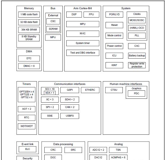
Figure 1. Block diagram of RA6M2
Evaluation Board EK-RA6M2 v1
Evaluation Kit for RA6M2 Microcontroller Group EK-RA6M2 v1
The EK-RA6M2 v1 enables developers to get started with initial firmware development.
• Renesas RA6M2 Microcontroller Group
R7FA6M2AF3CFB
144-pin LQFP package
120 MHz Arm® Cortex®-M4 core with Floating Point Unit (FPU)
384 KB SRAM
1 MB code flash memory
32 KB data flash memory
• Connectivity
A Device USB connector for the Main MCU
SEGGER J-Link® On-Board (OB) interface for debugging and programming of the RA6M2 MCU. A 10-pin JTAG/SWD interface is also provided for connecting optional external debuggers and programmers.
Two PMOD connectors, allowing use of appropriate PMOD compliant peripheral plug-in modules for rapid prototyping
Pin headers for access to power and signals for the Main MCU
• Multiple clock sources
Main MCU oscillator crystals, providing precision 12.000 MHz and 32,768 Hz external reference clocks Additional low-precision clocks are available internal to the Main MCU
• MCU reset push-button switch
• MCU boot configuration jumper
• General purpose I/O ports
One jumper to allow measuring of Main MCU current
Copper jumpers on PCB bottom side for configuration and access to selected MCU signals
• Operating voltage
External 5 V input through the Debug USB connector supplies the on-board power regulator to power logic and interfaces on the board. Alternatively, 5 V or 3.3 V may be supplied through alternate locations on the board.
• A two-color board status LED indicating availability of regulated power and connection status of the J-Link interface
• A red User LED, controlled by the Main MCU firmware
• A User Push-Button switch, User Capacitive Touch Sensor (button), and an optional User Potentiometer, all are controlled by the Main MCU firmware
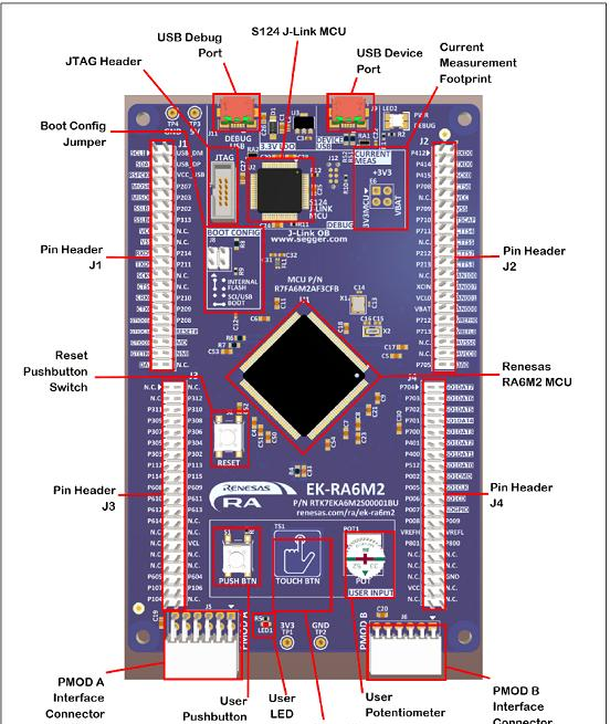
Figure 2. Outline drawing of the evaluation board EK-RA6M2 v1 (front)
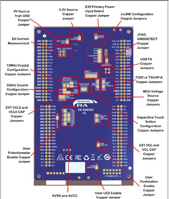
Figure 3. Outline drawing of the evaluation board EK-RA6M2 v1 (rear)
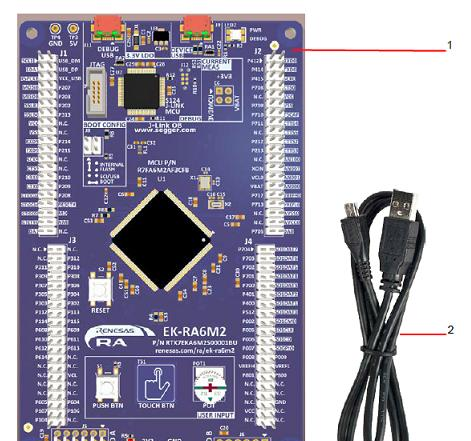
Figure 4. Outline drawing of the evaluation board EK-RA6M2 v1 (full set)
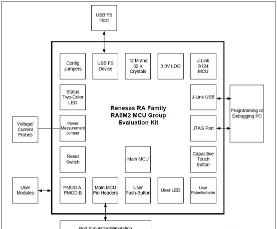
Figure 5. Block diagram of the evaluation board EK-RA6M2 v1
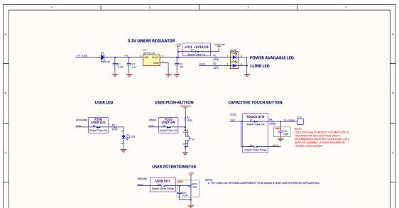
Figure 6. Evaluation board EK-RA6M2 v1 circuit diagram (1)
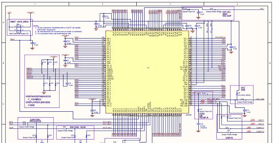
Figure 7. Evaluation board EK-RA6M2 v1 circuit diagram (2)

Figure 8. Evaluation board EK-RA6M2 v1 circuit diagram (3)
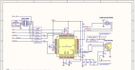
Figure 9. Evaluation board EK-RA6M2 v1 circuit diagram (4)
Evaluation board EK-RA6M2 v1 bill of materials:
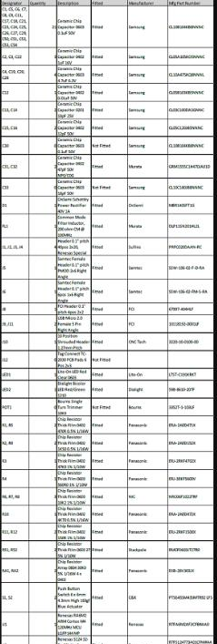
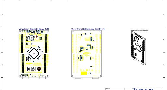
Figure 10. Evaluation board EK-RA6M2 v1 PCB design
责任编辑:David
【免责声明】
1、本文内容、数据、图表等来源于网络引用或其他公开资料,版权归属原作者、原发表出处。若版权所有方对本文的引用持有异议,请联系拍明芯城(marketing@iczoom.com),本方将及时处理。
2、本文的引用仅供读者交流学习使用,不涉及商业目的。
3、本文内容仅代表作者观点,拍明芯城不对内容的准确性、可靠性或完整性提供明示或暗示的保证。读者阅读本文后做出的决定或行为,是基于自主意愿和独立判断做出的,请读者明确相关结果。
4、如需转载本方拥有版权的文章,请联系拍明芯城(marketing@iczoom.com)注明“转载原因”。未经允许私自转载拍明芯城将保留追究其法律责任的权利。
拍明芯城拥有对此声明的最终解释权。


 产品分类
产品分类




 2012- 2022 拍明芯城ICZOOM.com 版权所有 客服热线:400-693-8369 (9:00-18:00)


